Lab 7: Operational Amplifiers
ECE203 - Electrical Circuits II
Electrical and Computer Engineering - University of Alberta
1 Objectives
In this lab session, you will be introduced to a common electronic component known as the Operational Amplifier, or op amp for short. Operational amplifiers are linear devices that have all the properties required for nearly ideal DC amplification and are therefore used extensively in signal conditioning, filtering or to perform mathematical operations such as add, subtract, integration and differentiation. The objectives of this lab are to introduce the following circuits and some of their characteristics:
- Inverting Op Amp Amplifier circuit
- Change the value of the feedback resistor (Rf) to see how it effects gain.
- Change the magnitude of the input voltage to see where its operation is linear.
- Operate the amplifier under a large range of frequencies to see how it effects gain.
- Measure the input resistance of the inverting amplifier.
- Measure the output resistance of the operational amplifier.
- Non-inverting Op Amp Amplifier circuit
- Change the value of the feedback resistor (Rf) to see how it effects gain.
- Measure the input resistance of the non-inverting amplifier.
1.1 Equipment Required
- The Lab 7 - Results sheet to record your measurements.
- A Computer with Waveforms installed
- Analog Discovery 2
- Breadboard Breakout for the Analog Discovery 2 with a ribbon cable
- USB A to Micro-B cable
- Digital multimeter
- MB102 breadboard
- Jumper wires
- uA741 - Operational Amplifier - datasheet
- The following Resistors (1/4 watt, 1% or 5%)
- 470Ω
- two - 1kΩ
- two - 4.7kΩ
- 10kΩ
- 20kΩ
1.2 Background
Ideal Opamp
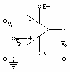
The Opamp
The inputs and outputs of the operational amplifier are as follows:
- Vn: the inverting input
- Vp: the non-inverting input
- E+, E-: input terminals for the DC power supply required for amplification
- VO: the output terminal
When there is a difference between Vn and Vp, amplification occurs, and
\[V_O = A(V_n-V_p)\]
An ideal op amp has the following characteristics:
- Voltage gain: A = ∞
- Bandwidth: BW = ∞
- Input resistance: Rin = ∞
- Output resistance: Rout = 0
- when (Vn = Vp) means that VO = 0
Real Opamp
Commercial op amps closely approximate these ideal characteristics, so most analytic expressions for practical circuits in the kHz range use these ideal characteristics plus some very important axioms.
Axiom 1: because A = ∞, any output signal Vo will be the result of an infinitesimally small input signal. In essence, therefore, for analog operation: Vn – Vp = 0. This says that the differential input voltage is zero.
Axiom 2: because Rin = ∞, there is no current flow into either input terminal of the op amp.
When an op amp is placed in a circuit, it is usually wired so that the output voltage is “fed back” to the input circuit. The axioms mentioned above will be used with circuit solving techniques to predict the output voltage. The op amp configurations used in this lab are described below.
Bandwidth and Saturation
As was mentioned earlier, an op amp provides linear amplification of input voltages over a range. The two factors that can contribute to non linear amplification are:
- The frequency of the input signal (Bandwidth).
- The voltage level of the input signal (Saturated).
Bandwidth
The bandwidth of the amplifier is range of input frequencies for which the amplification is linear, or nearly so. The bandwidth BW is defined as the frequency interval within which:\[A_f > \frac{A_f \textrm{(ideal)}}{\sqrt{2}}\]
Saturation
The op amp is said to be saturated when the input signal is too large to be amplified by the predicted value. This is limited by the DC power supply to the op amp, and the idea that an op amp cannot produce more voltage than it is supplied.
2 Procedures
Setup the Analog Discovery 2 as done in the previous labs.
Connect the USB cable from the Analog Discovery 2 your computer.
Use the ribbon cable and 15x2 header pins to connect the Analog Discovery 2 to your Breadboard Breakout . Make sure that the orange wires of the ribbon cable end up on the same side as the breadboard breakout pin labeled 1+.
Plug the breadboard breakout into the breadboard.
Launch the Waveforms software making sure that it detects your Analog Discovery 2.
Placing the Operational Amplifier IC on the Breadboard.
- The op amp comes in a common IC package known as a 8-pin DIP package and looks like the following. Note that the IC has a small circle in one of the corners to indicate which pin is pin 1.

- From the uA741 datasheet here is how the physical package relates to the schematic interpretation of the op amp with a description of all the pins.
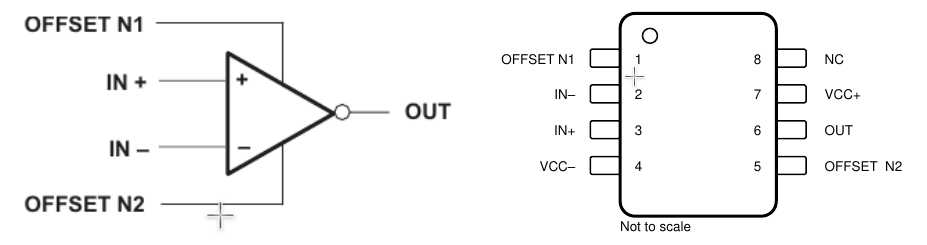
- Place the op amp on the breadboard as shown below. The breadboard is designed to accept these kinds of IC’s with them straddling the center divider.

2.1 Inverting Amplifier
Inverting amplifier
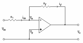
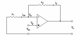
The Inverting Amplifier
In this circuit, Vp is grounded and the input signal is fed in via R1. Because of Axiom 1, Vn is equal to zero as well. All of Vin appears across R1.
All of this input current flows through Rf (because of Axiom 2) so iin = if.
\[i_{in} = \frac{V_{in}}{R_1} \qquad = \qquad i_f \frac{-V_O}{R_f}\]
Rf is called the feedback resistor. A portion of the output signal is fed back from VO to Vn via Rf. Since Vn is approximately ground, then all of the output voltage appears across Rf. Equating the two currents above gives:
\[\frac{V_{in}}{R_1} = \frac{-V_O}{R_f}\]
This implies that:
\[\frac{V_O}{V_{in}} = \frac{-R_f}{R_1} = A_f\]
Af is the feedback gain of the inverting amplifier, and it may be varied by changing either Rf or R1.
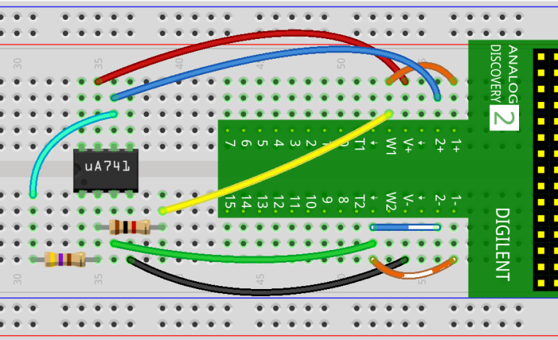
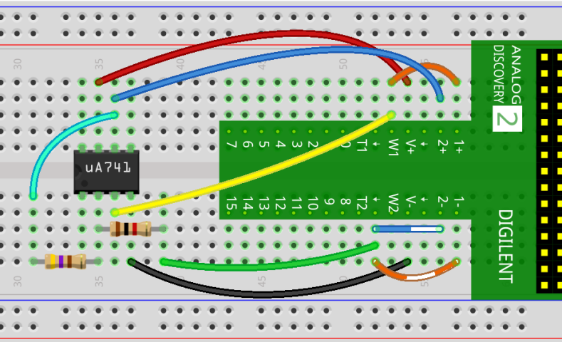
Connect the circuit below using the following:
- To power the operational amplifier we first have to supply it with
power from the Analog Discovery 2s’ DC power supplies:
- Connect the VCC+ pin (pin 7) of the op amp to the V+ of the Analog Discovery 2.
- Connect the VCC- pin (pin 4) of the op amp to the V- of the Analog Discovery 2.
- A 1kΩ resistor for R1, connect one end to the IN- pin (pin 2) and the other to the W1 output of the Analog Discovery 2. You might also need to use a jumper wire to make the connection as the resistor might not be long enough.
- Starting with a 470Ω resistor for Rf, connect one end to the IN- pin (pin 2) and the other to the OUT pin (pin 6). You might also need to use a jumper wire to make the connection over to the other side of the op amp.
- Connect the IN+ pin (pin 3) to the ground connection of the Analog Discovery 2.
- To measure Vin use jumper wires to connect Wavegen (W1) to the channel 1 inputs of the Analog discovery 2 by connecting W1 to 1+ and ground to 1-.
- To measure Vout use jumper wires to connect the output of the amplifier to the channel 2 inputs of the Analog Discovery 2 by connecting Vout to 2+ and ground to 2-.
- Leave all of the other op amp pins disconnected.
- To power the operational amplifier we first have to supply it with
power from the Analog Discovery 2s’ DC power supplies:

Figure 1. Inverting Op Amp
Click here
to see a simulation
demo of this circuit.
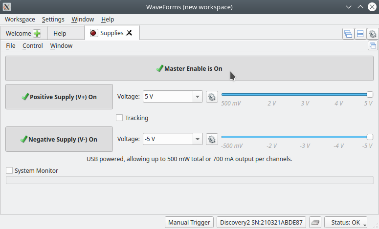
- In Waveforms start the Supplies tool and configure it to output 5 V on the Positive Supply (V+) and -5 V on the Negative Supply (V-). Once configured enable all of the supplies so they output the corresponding voltage on the pins to power the op amp.
With the Supplies still running in Waveforms also start the Wavegen tool and configure it with the following settings and once complete click on the ‘Run’ button to output the waveform on the W1 pin.
- Type: Sine
- Frequency: 5 kHz
- Amplitude: 100 mV
- Offset: 0 V
- Symmetry: 50 %
- Phase: 0 °
With both the Supplies and Wavegen running open up the Scope tool in Waveforms and ‘Run’ it. Adjust the Scope setting until you obtain a display that looks similar to the one below.
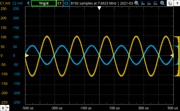
Note:
Vin is the Yellow waveform and Vout is the Blue waveform. The waveforms are ideally identical but inverted and with the gain applied. If you would like you can play with the Wavegen and output different amplitudes, frequencies and even different waveform types to see the result. Make sure to reset everything to the original settings before moving on.
- Use the ‘Measurements’ tool in the Scope to automatically measure the peak-to-peak amplitude of both channel 1 (Vin) and channel 2 (Vout). Remember that when making automatic measurements the quality of the measurement is only as good as the waveform on the display. Therefore try and have the magnitude of the waveform fairly large on the screen without running into the maximum or minimum of the display. It is also good practice to have somewhere between two and ten cycles of the waveform shown on the display. If this isn’t followed large errors can occur in your measurements.
2.1.1 Changing Rf
While keeping the input voltage (Vin) constant at 100mVpeak at 5kHz and leaving in the 1kΩ resistor for R1, measure the peak-to-peak voltage for both Vin and Vout when you switch the Rf resistor to the following values. For each input voltage measure and record your results in the appropriate place on the results sheet.
- Rf = 470Ω
- Rf = 1kΩ
- Rf = 4.7kΩ
- Rf = 10kΩ
- Rf = 20kΩ
Note:
The ideal gain for a Inverting amplifier is calculated with the following formula: \[Af = -\frac{Rf}{R1}\] Typically to indicate that the output voltage is 180 degrees out of phase with the input voltage a minus sign is used to describe the gain of an amplifier.
2.1.2 Increasing Vin
With R1 still at 1kΩ and the Rf resistor set to 4.7kΩ adjust the input voltage (Vin) using the Wavegen tool to the following magnitudes while keeping the frequency at 5kHz. For each magnitude record the input voltage (Vin) and output voltage (Vout) in the appropriate place on the results sheet.
- Vin = 50 mVpeak
- Vin = 100 mVpeak
- Vin = 200 mVpeak
- Vin = 500 mVpeak
- Vin = 1 Vpeak
- Vin = 2 Vpeak
2.1.3 Increasing Frequency
With R1 still at 1kΩ and the Rf resistor set to 4.7kΩ adjust the frequency of the input voltage using the Wavegen tool to the following while keeping the magnitude of Vin at 500mVpeak. For each frequency measure and record the input voltage (Vin) and output voltage (Vout) in the appropriate place on the results sheet.
- f = 100 Hz
- f = 300 Hz
- f = 1 kHz
- f = 3 kHz
- f = 10 kHz
- f = 30 kHz
- f = 100 kHz
- f = 300 kHz
- f = 1 MHz
- f = 3 MHz
2.1.4 Input Resistance
To determine the input resistance of the Inverting amplifier we need to modify the circuit as shown below:
- R1 = 1 kΩ, Rf = 4.7 kΩ
- Insert a Rsense resistor from the list below (beginning with the
470Ω) between the Wavegen output and the R1 resistor of the amplifier.
- Rsense = 470 Ω
- Rsense = 1 kΩ
- Rsense = 4.7 kΩ
- Use the Channel 2 scope input to measure the output voltage (VW1) from the Analog Discovery 2s’ Wavegen.
- Use the Channel 1 scope input to measure the input voltage (Vin) to the Inverting amplifier.

Figure 2. Measure Input Resistance
Set the Wavegen to output a 500mVpeak sinewave at 5kHz.
Use the automatic measurements you created earlier in the Scope to measure the peak-to-peak voltage amplitudes of both Channel 2 (VW1) and Channel 1 (Vin). Record your measurements in the appropriate place on the results sheet.
Replace the Rsense resistor, first with the 1 kΩ and then the 4.7 kΩ, and repeat the measurement from the previous step. Record your measurements in the appropriate place on the results sheet.
Before proceeding to the next section restore your circuit by completely removing the Rsense resistor and reconnecting the Wavegen to the input voltage (Vin) of the Amplifier. Also remove the Channel 2 Scope inputs from the Wavegen and place them back across the Amplifiers output voltage (Vout).
2.1.5 Output Resistance
As the output resistance of the Inverting amplifier is too small for us to measure using the equipment we have available. We will simply measure the output resistance of the op amp instead. To determine this output resistance we need to modify the circuit as shown below:
- R1 = 1 kΩ, remove the feedback resistor Rf.
- Insert a Rload resistor from the list below, beginning with an open
load.
- Rload = open or ∞ Ω
- Rload = 470 Ω
- Rload = 1 kΩ
- Rload = 4.7 kΩ
- Make sure that the Channel 2 Scope is connected to measure the output of the op amp.

Figure 3. Measure Output Resistance
Adjust the Wavegen to output the following.
- Type: DC
- Offset: 5 V
Using the ‘Measurements’ tool of the Scope add a ‘DC RMS’ measurement for channel 2 to determine the magnitude of the output voltage. Record this voltage as the open circuited output of the op amp in the appropriate place on the results sheet.
First add a Rload resistor of 470Ω, then 1 kΩ and 4.7kΩ, to the op amp circuit and measure the new output voltage for each value of Rload resistor. Make sure to record your measurements in the appropriate place on the results sheet.
Note:
The specified output resistance of the uA741 op amp can be found on the uA741 datasheet on page 6 as ro.
2.2 Non-inverting Amplifier
Non-inverting amplifier
The Non-Inverting Amplifier
An input signal Vin is applied to the non-inverting input Vp. Axiom 1 and Axiom 2 tell us that the voltage across R1 is equal to the voltage Vin. Also from Axiom 2, iin = if.
\[i_{in} = \frac{-V_{in}}{R_f} \qquad = \qquad i_f = \frac{V_{in}-V_O}{R_f}\]
Rearranging the above equation gives the expression for the feedback gain (Af) of the non inverting amplifier. The voltage amplification of this amplifier is:
\[\frac{V_O}{V_{in}} = \frac{R_1+R_f}{R_1} = Af\]
Start over or modify your previous circuit to create the circuit as shown below:
- Power the op amp with the same +5V and -5V supplies as before.
- Connect the IN+ pin (pin 3) to the Wavegen output (W1) of the Analog Discovery 2.
- A 1kΩ resistor for R1, connect one end to the IN- pin (pin 2) and the other to the ground of the Analog Discovery 2. You might also need to use a jumper wire to make the connection as the resistor might not be long enough.
- Starting with a 470Ω resistor for Rf, connect one end to the IN- pin (pin 2) and the other to the OUT pin (pin 6). You might also need to use a jumper wire to make the connection over to the otherside of the op amp.
- To measure Vin use jumper wires to connect the Wavegen output to the channel 1 inputs of the Analog discovery 2 by connecting W1 to 1+ and ground to 1-.
- To measure Vout use jumper wires to connect the output of the amplifier to the channel 2 inputs of the Analog Discovery 2 by connecting OUT (pin 6) to 2+ and ground to 2-.
- Leave all of the other op amp pins disconnected.

Figure 4. Non-inverting op amp
Click here
to see a simulation
demo of this circuit.
As before, make sure the Supplies tool in Waveforms is configured to output 5 V on the Positive Supply (V+) and -5 V on the Negative Supply (V-). Once it is configured enable all of the supplies so they output the corresponding voltage on the pins to power the op amp.
Again as before, with the Supplies still running in Waveforms also start the Wavegen tool and configure it with the following settings and once complete click on the ‘Run’ button to output the waveform on the W1 pin. Make sure reset the Offset to 0V as you changed it during the last section.
- Type: Sine
- Frequency: 5 kHz
- Amplitude: 100 mV
- Offset: 0 V
- Symmetry: 50 %
- Phase: 0 °
Yet again as before, open the Scope tool and ‘Run’ it with both the Supplies and Wavegen also continuing to run. Adjust the Scope setting until you obtain an appropriate display. Use the ‘Measurement’ tool to automatically measure the peak-to-peak amplitudes of both channel 1 (Vin) and channel 2 (Vout).
2.2.1 Changing Rf
While keeping the input voltage (Vin) constant at 100mVpeak at 5kHz and leaving in the 1kΩ resistor for R1, measure the peak-to-peak voltage for both Vin and Vout when you switch the Rf resistor to the following values. For each input voltage measure and record your results in the appropriate place on the results sheet.
- Rf = 470Ω
- Rf = 1kΩ
- Rf = 4.7kΩ
- Rf = 10kΩ
- Rf = 20kΩ
Note:
The ideal gain for a Non-inverting amplifier is calculated with the following formula: \[Af = 1+\frac{Rf}{R1}\]
2.2.2 Input Resistance
To determine the input resistance of the Non-inverting amplifier we need to modify the circuit in a similar fashion as we did for the Inverting Amplifier:
- R1 = 1 kΩ, Rf = 4.7 kΩ
- Rsense = 20kΩ
- Use the Channel 2 scope input to measure the output voltage (VW1) from the Analog Discovery 2s’ Wavegen.
- Use the Channel 1 scope input to measure the input voltage (Vin) to the Non-inverting amplifier.

Figure 5. Measure Input Resistance
Set the Wavegen to output a 4Vpeak sinewave at 5kHz.
Use the automatic measurements you created earlier in the Scope to measure the peak-to-peak voltage amplitudes of both Channel 2 (VW1) and Channel 1 (Vin). Record your measurements in the appropriate place on the results sheet.
Note:
The specified input resistance of the uA741 op amp can be found on the uA741 datasheet on page 6 as ri.
2.3 Cleanup
Congratulations, you have completed the experimental part of the the laboratory. Before cleaning up, I’d suggest going through your results to check that you have completed everything and that your results make sense. If you find any issues, I’d suggest resolving or making a note of it now. If you are not continuing to work with the equipment please disconnect everything and put it away to prevent it from getting damaged.
3 Post Lab
The following is what you are expected to complete and submit for grading for Lab 7 before the deadline.
The completed Lab 7 - Results sheet template provided at the beginning of this lab manual under Equipment required. This sheet should include the following:
- Your name, student ID and CCID.
- All of the required measurements from the lab procedures.
- All of the required calculations as discussed below.
- The required plots as discussed below.
The Lab 7 - Results sheet needs to be submitted to the Submit (Lab 7 - Results) link on eClass as a pdf document .
- Complete the online Quiz (Lab 7 - Post Lab) on eClass.
3.1 Calculations
For these calculation you only need to provide the answers in the space provided on your results sheet, you do not need to show your work.
Calculate the ideal gain of each of the op amp amplifier circuits based on the resistor network connected to them. Include your calculation results in the appropriate place on the results sheet.
From your measured input and output voltage calculate the actual gain of each of the op amp amplifier circuits. Include your calculation results in the appropriate place on the results sheet.
To determine the input resistance of each of the amplifier circuits use the following procedures.

- First calculate the voltage across the Rsense resistor using the following equation.
\[V_{Rsense} = V_{W1} - V_{V_{IN}}\]
- Then calculate the current throught the Rsense resistor by using ohms law. Note the current through the Rsense resistor is equivalent to the current going into the input of the amplifier.
\[I_{IN} = \frac{V_{Rsense}}{Rsense}\]
- Lastly, use the input voltage and the input current into the amplifier to calculate the input resistance.
\[R_{IN} = \frac{V_{IN}}{I_{IN}}\]
To determine the output resistance of the uA741 operational amplifier for each Rload resistor use the following procedures:

- Calculate the output current through the connected load resistor (Rload) using the following. Note the current through the output resistor equals the current coming out of the op amp.
\[I_{OUT} = \frac{V_{OUT}}{R_{Load}}\]
- Than calculate the voltage drop across output resistance (Rout) by taking the open circuit output voltage and subtracting the voltage when the load resistor is connected.
\[V_{Rout} = V_{OUT}^{open} - V_{OUT}^{Rload}\]
- Finally to calculate the output resistance use the following:
\[R_{OUT} = \frac{V_{Rout}}{I_{OUT}}\]
3.2 Plots
To create your plots you can use whichever software you would like (Excel, Matlab, etc), export your plot as an image and import it into your Lab 7 - Results sheet in the appropriate place.
Your plots should include:
- A Plot title
- Label your axes and show what unit of measure is used.
- Include a marking for your datapoints.
- Include a line between your datapoints in the same series.
- Include a legend.
- Make sure your scales are appropriate and visible.
Note:
When plotting the gain and ideal gain for the inverting amplifier use the absolute value.
Inverting Amplifier - Changing Rf: Plot both the measured gain and ideal gain vs. the feedback resistance (Rf).
Inverting Amplifier - Increasing VIN: Plot both the measured gain and ideal gain vs. the input voltage (Vin).
Inverting Amplifier - Increasing f: Plot both the measured gain and ideal gain vs. the applied frequency (f) – Use a log scale for the x axis.
Non-inverting Amplifier - Plot both the measured gain and ideal gain vs. the feedback resistance (Rf).
3.3 Questions
Complete the online Quiz (Lab 7 - Post Lab) on eClass.