Lab 8: Diodes
ECE203 - Electrical Circuits II
Electrical and Computer Engineering - University of Alberta
1 Objectives
In this lab session, you will be introduced to another common electronic component known as the diode. A diode is a semiconductor device that essentially acts as a one-way valve for current. It allows current to flow easily in one direction, but severely restricts current from flowing in the opposite direction. The objectives of this lab are to introduce the diode and a few of its most common uses.
Measure the typical Diode operating characteristics
Two simple diode rectifier circuits
- Half-wave
- Full-wave bridge
A biased positive shunt clipper circuit.
1.1 Equipment Required
- The Lab 8 - Results sheet to record your measurements.
- Print out and bring a copy of the Lab 8 - Sketchbook to draw the conduction angle waveforms and show the conduction angle calculations.
- A Computer with Waveforms installed
- Analog Discovery 2
- Breadboard Breakout for the Analog Discovery 2 with a ribbon cable
- USB A to Micro-B cable
- Digital multimeter
- MB102 breadboard
- Jumper wires
- four 1N4005 Diodes - datasheet
- The following Resistors (1/4 watt, 1% or 5%)
- 100Ω
- 1kΩ
2 Procedures
Setup the Analog Discovery 2 as done in the previous labs.
Connect the USB cable from the Analog Discovery 2 your computer.
Use the ribbon cable and 15x2 header pins to connect the Analog Discovery 2 to your Breadboard Breakout . Make sure that the orange wires of the ribbon cable end up on the same side as the breadboard breakout pin labeled 1+.
Plug the breadboard breakout into the breadboard.
Launch the Waveforms software making sure that it detects your Analog Discovery 2.
2.1 DMM Diode test
A multimeter’s Diode Test mode produces a small voltage between test leads. The multimeter then displays the voltage drop of the diode when the test leads are connected across a forward-biased diode and an over limit (OL) when connected across a reverse biased diode. The Diode Test procedure is conducted as follows:
Make certain that:
- All power to the circuit is OFF.
- No voltage exists at the diode. Voltage may be present in the circuit due to charged capacitors. If so, the capacitors need to be discharged. Set the multimeter to measure ac or dc voltage as required.
- There is no other component in parallel with the diode that will effect the measurement. If this is the case it might be necessary to remove one end of the diode from the circuit.
Turn the dial (rotary switch) to Diode Test mode. It may share a space on the dial with another function.
Connect the test leads to the diode to measure the forward-biased voltage. For a good silicon diode the reading should be in the 0.5V to 0.8V range.
Reverse the test leads to measure the reverse bias. For a good diode the DMM should measure ‘OL’ (over limit) which means the circuit is open and no current is flowing.

Diode test analysis
A good forward-based diode displays a voltage drop ranging from 0.5 to 0.8 volts for the most commonly used silicon diodes. Some germanium diodes have a voltage drop ranging from 0.2 to 0.3 V.
The multimeter displays OL when a good diode is reverse-biased. The OL reading indicates the diode is functioning as an open switch.
A bad (opened) diode does not allow current to flow in either direction. A multimeter will display OL in both directions when the diode is opened.
A shorted diode has the same voltage drop reading (approximately 0.4 V) in both directions.
Use the multimeter to measure both the forward and reverse bias of the 1N4005 diodes included in your kit.

2.2 Diode Characteristics
Ideal Diode
A diode is a two terminal device, represented as follows:
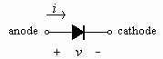
Figure 8.1: A Diode
There are two different cases for diode operation:
Forward biased (turned on): If a current is applied in the direction shown in Figure 8.1 to the diode, the diode acts like a short circuit and the voltage drop across it is zero (in the ideal scenario).
Reverse biased (turned off): If a voltage is applied across a diode, negative to the reference voltage shown in Figure 8.1, the diode acts like an open circuit and does not conduct any current.
The response of the diode to forward and reverse biasing gives it its unusual i-v characteristic, illustrated in Figure 8.2:
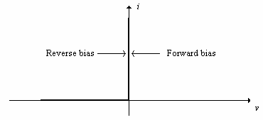
Figure 8.2: i-v Characteristic of a Diode
Non-Ideal Characteristics
As mentioned briefly above, an actual diode will not operate exactly as predicted in theory. Although a forward biased diode was previously described to act as a short circuit, it will actually have a small but significant voltage drop across it, around 0.6V. The consequences of this are:
A diode does not conduct as soon as there is a positive voltage across it. It will instead conduct when the forward voltage exceeds 0.6V.
Rectifier circuits can never completely recover the energy of the input source. Some power will always be dissipated in the diode.
Conduction Angle
The conduction angle is defined as the amount of a period a device conducts as an angle relative to a complete cycle (ie. 360°).
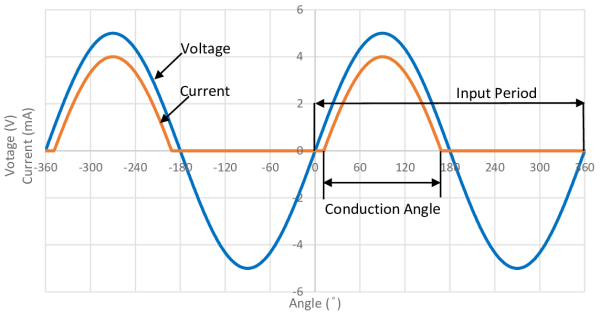
Figure A1: Conduction angle for a diode
Connect the circuit below on the breadboard using the following:
- Use the channel 1 (W1) ‘Wavegen’ outputs to supply a voltage to a 1N4005 diode in series with a 1kΩ resistor. Make sure the diode is pointing in the same direction as in the schematic.
- Use the channel 1 ‘Scope’ inputs to measure the voltage across the Wavegen (W1).
- Use the channel 2 ‘Scope’ inputs to measure the voltage across the Resistor (R1).

Figure 1. Diode Characteristics Circuit
Click here
to see a simulation
demo of this circuit.
In ‘Waveforms’ start the Wavegen tool and configure it with the following settings and once complete click on the ‘Run’ button to output the waveform to your circuit.
- Type: Triangle
- Frequency: 100 Hz
- Amplitude: 2 V
- Offset: 0 V
- Symmetry: 50 %
- Phase: 0 °
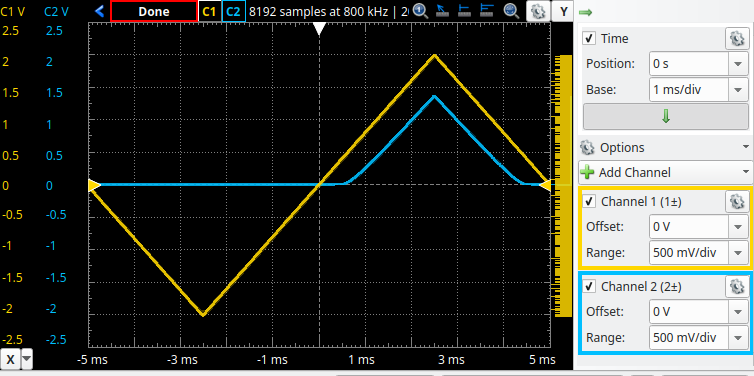
With the Wavegen in Waveforms still running also open up the Scope tool and run it as well. Adjust the controls if necessary until you obtain similar waveforms to the two below. The yellow is the source (Wavegen) voltage and the blue is the resistor voltage.
Create a new math channel to determine the voltage across the diode (VD). To do this select ‘Add Channel’ then ‘Simple’ and make the equation in the Math 1 box read ‘C1 - C2’. We can do this to determine the diode voltage because of Kirchhoff’s voltage law.
Create another new math channel to determine the current through the diode (ID). To do this select ‘Add Channel’ then ‘Custom’ and enter the following equation in the available text box ‘C2/1000’ and change the ‘Units’ to ‘A’. We can do this to determine the current because of ohms law and the resistor is 1kΩ. Once the 2 new math channels are added you may disable channel 1 and 2 for a moment as we are not concerned with measuring them. Adjust the controls if necessary until you obtain similar waveforms to the two below. The red is the diode voltage (VD) and the dark blue is the diode current (ID).

Use the ‘X Cursors’ in the scope to measure the forward biased diode voltages at the following approximate diode currents: 250uA, 500uA, 750uA, 1000uA and 1250uA. Feel free to adjust any of the Scope settings to obtain good measurements. Record your measurements in the appropriate place in the results sheet.
Again use the ‘X Cursors’ to measure the reverse biased diode currents at the following approximate diode voltages: 0V, -0.5V, -1V, -1.5V and -2V. Feel free to adjust any of the Scope settings to obtain good measurements. Record your measurements in the appropriate place in the results sheet.
Since we are measuring both the diode voltage (VD) and the diode current (ID) simultaneously we can use one of the scopes tools to automatically create the diodes characteristic curve. This tool will plot one of the input channels against the other input channel to display what is called an XY plot. To do this select the ‘+XY’ tool in the Scopes top toolbar and then select ‘M1’ for ‘X’ and ‘M2’ for ‘Y’. You should have something that looks similar to the plot below.
2.3 Rectifier Circuits
AC signals will be altered in circuits with diodes, because the diode will only conduct in one direction. This section investigates the effect of half and full wave rectifiers on an AC signal.
2.3.1 Half-wave
Half-wave Rectifier
A simple circuit with one diode in it, like in Figure 8.3, can be used to reject one half of an alternating voltage source, introducing an average value (a DC component) into the output voltage.
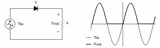
Figure 8.3: A Half Wave Rectifier and its Output Voltage
The output waveform shown is for an ideal diode. In reality, there is a drop of about 0.6V across a forward biased diode, causing the waveform representing VOUT to be slightly smaller than VIN.
Average Output
The average output of a diode cycle gives insight into how well the rectifier circuit is converting AC to DC.
The average value of the output tells how much of the signal is not being absorbed in the diode. By comparing the ratio of average output to RMS input, one can tell which circuit is more efficient. To find an approximation of the average value of the output:
- The output peak is approximated as a sine curve of amplitude (VPeak – VDO). This is not entirely accurate, but is sufficient for our purposes.
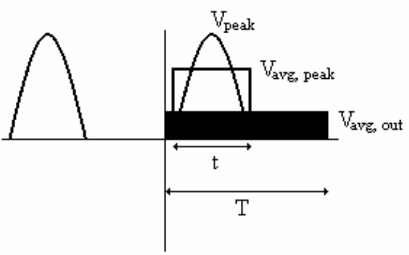
Figure A2: The Average Value of a Half Rectified Signal
- The average value of a sinusoidal peak is:
\[V_{avg, peak} = \frac{V_{Peak}}{\sqrt{2}}\]
This is the value, when multiplied by the period of the peak (t in Figure A2), that gives the area as the area under the peak.
- The average of the output over the whole period is the value that, when multiplied by the period of the input waveform (T in Figure A2), gives the same area as the area under the peak. This is determined by:
\[V_{avg} = \frac{V_{avg,peak} \times t}{T}\]
The circuit below is the same circuit used in the previous section. The only difference is that now we are going to apply a 5VPeak Sinewave and compare the input voltage to the output voltage. Make the following changes to the Wavegen:
- Type: Sine
- Amplitude: 5V

Figure 2. Half-wave Diode Rectifier Circuit
Click here
to see a simulation
demo of this circuit.
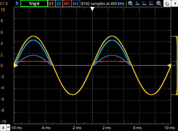
- Using the same Scope setup from the previous section adjust the Scope ranges so the resulting waveforms can be displayed properly. It should look like something like below where the yellow waveform is the input voltage (VIN), the light blue is the output voltage (VOUT), the red is the diode voltage (VD), and the dark blue is the current (ID).
Use either the ‘Y Cursors’ or the ‘Measurement’ tool in the Scope to determine the peak amplitudes of the input voltage, output voltage and diode voltage. Record your measurements in the appropriate place in the results sheet.
Use the ‘Measurement’ tool to determine the ‘Average’, ‘AC RMS’ and ‘DC RMS’ of the input voltage and output voltage. Record you measurements in the appropriate place in the results sheet.
Measure and record the unknown quantities associated with calculating the conduction angle of the half-wave diode rectifier in the appropriate place on the results sheet. Include an appropriate measurement title, the units used and your measured quantity.
On the printed sketchbook sheet, clearly draw two cycles of the relevant half-wave diode rectifier conduction angle waveforms and then draw cursors to indicate the relevant quantities you measured in the previous step. Make sure to add axes titles, labels, units, and the relevant measured values. Also, show your calculation of the half-wave diode rectifiers conduction angle in the space provided on the page using your measured values. Place your result in the appropriate place on the results sheet.
2.3.2 Full-wave (Bridge)
Full-wave (Bridge) Rectifier
This circuit is more complicated than a simple half wave rectifier; it requires four diodes hooked up in bridge formation, as illustrated in Figure 8.4. The advantage that is has is that for both the positive and negative halves of the input voltage cycle, there is a path through two forward biased diodes and a resistor, to give an output voltage. Study of Figure 8.4 reveals that the current will always pass through the positive terminal of the resistor, so the output voltage will be as shown.
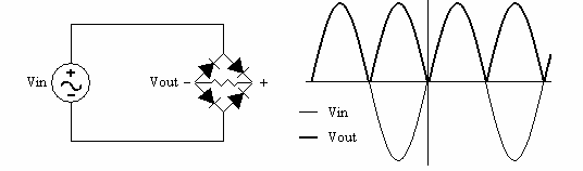
Figure 8.4: A Bridge Rectifier and its Output Voltage
The output waveform is shown for an ideal diode. In reality, there will be two voltage drops, one for each of the forward biased diodes the current will pass through, so the output waveform will once again be smaller than the input.
How much the non-ideal characteristic of a diode affects the performance of a rectifier can be measured in two ways. The conduction angle (the fraction of one entire cycle of the input voltage that the diode conducts) can be calculated, and the average value of the output (DC component) can be calculated. Comparing these values for different circuits can help a designer decide which circuit is best for their purposes.
Average output
The procedure is nearly the same for a bridge rectified circuit. This time around there are two peaks per cycle, and each will probably have a different peak value, so more work is required.
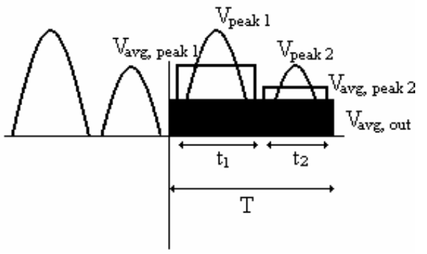
Figure A3: The Average Value of a Bridge Rectified Signal
Each peak is approximated as a sine curve with the amplitude measured.
The average value of each peak is determined in the same way as before:
\[V_{avg, peak} = \frac{V_{Peak}}{\sqrt{2}}\]
- The average value of the output over the whole period is the value that, when multiplied by the period of the input waveform, gives the same area as the total area under the two peaks.
\[V_{avg,out} = \frac{V_{avg,peak1}\times t_1 + V_{avg,peak2 \times t_2}}{T}\]
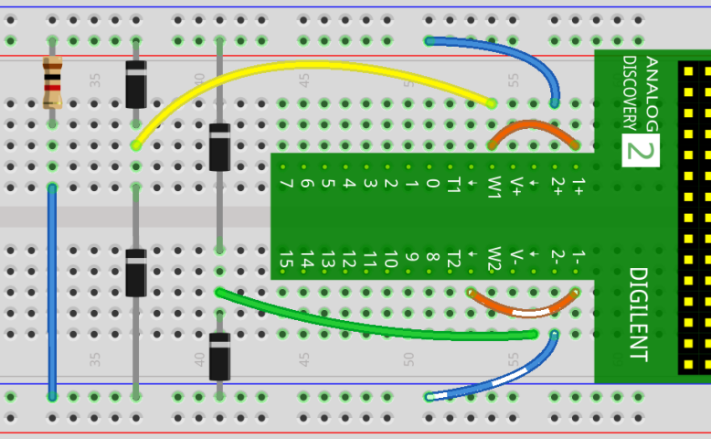
Connect the circuit below using the following:
- Use four 1N4005 diodes to form a bridge as shown on the breadboard diagram below.
- Use a 1kΩ resistor to add a load current to the diode bridge.
- Use the channel 1 (W1) ‘Wavegen’ outputs to supply a voltage to the diode bridge.
- Use the channel 1 ‘Scope’ inputs to measure the input voltage (VIN) across the Wavegen (W1).
- Use the channel 2 ‘Scope’ inputs to measure the output voltage (VOUT) across the Resistor (R1).
Note:
The input and output do not share a common ground point.

Figure 3. Full-wave Diode Rectifier Circuit
Click here
to see a simulation
demo of this circuit.
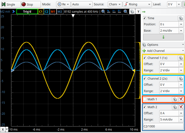
- Using the same 5VPeak@100Hz Sinewave for the input voltage and adjusting the Scope setting appropriately from the last section. You should obtain something that looks like the following: Where the yellow waveform is the input voltage (VIN), the light blue is the output voltage (VOUT), the red is no longer applicable, and the dark blue is the load current through the resistor.
Use either the ‘Y Cursors’ or the ‘Measurement’ tool in the Scope to determine the peak amplitudes of the input voltage, output voltage and diode voltage. Record your measurements in the appropriate place in the results sheet.
Use the ‘Measurement’ tool to determine the ‘Average’, ‘AC RMS’ and ‘DC RMS’ of the input voltage and output voltage. Record you measurements in the appropriate place in the results sheet.
Measure and record the unknown quantities associated with calculating the conduction angle of the full-wave diode rectifier in the appropriate place on the results sheet. Include an appropriate measurement title, the units used and your measured quantity.
On the printed sketchbook sheet, this time for the full-wave diode rectifer, clearly draw two cycles of the relevant conduction angle waveforms and then draw cursors to indicate the relevant quantities you measured in the previous step. Make sure to add axes titles, labels, units, and the relevant measured values. Also, show your calculation of the full-wave diode rectifiers conduction angle in the space provided on the page using your measured values. Place your result in the appropriate place on the results sheet.
2.4 Clipping Circuits
Clipping circuits
It is sometimes desirable to keep the output voltage of a circuit to within upper or lower bounds. Variations of this can be achieved using any of the circuits shown below:
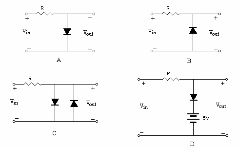
Figure 8.5: Clipper Circuits
While the value of Vin is less than the forward voltage required to turn the diode on, no current flows and the output voltage is the same as the input voltage.
However, once the diode has been turned on, the voltage drop across it is constant and equal to the barrier voltage. Even if the input voltage increases, the output voltage will not. The transfer characteristics for circuits A and B are given in Figure 8.6.
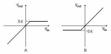
Figure 8.6: Transfer Characteristics
2.4.1 Biased Positive Shunt Clipper
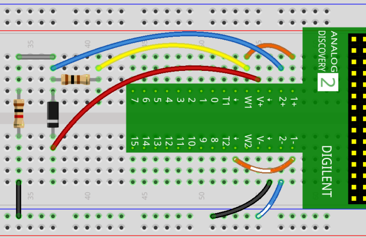
Connect the circuit below using the following:
- Use a 1N4005 diode for D1 in series with the positive DC power supply from the Analog Discovery 2 to create the clipper. Make sure the diode is in the correct orientation.
- Use a 100Ω resistor for R1 to limit current coming out of the Analog Discovery 2’s Wavegen.
- Use a 1kΩ resistor for RL to load the circuit.
- Connect the Wavegen to supply a voltage to the input of the clipper circuit.
- Use the channel 1 ‘Scope’ inputs to measure the input voltage (VIN) across the Wavegen (W1).
- Use the channel 2 ‘Scope’ inputs to measure the output voltage (VOUT) across the Resistor (RL).

Figure 4. Biased Positive Shunt Clipper Circuit
Click here
to see a simulation
demo of this circuit.
Configure the Wavegen tool with the following settings and once complete click on the ‘Run’ button to output the waveform to your circuit.
- Type: Triangle
- Frequency: 100 Hz
- Amplitude: 2 V
- Offset: 2 V
- Symmetry: 50 %
- Phase: 0 °
With the Wavegen in Waveforms still running use the Scope to measure the output voltage (VOUT) when the input voltage (VIN) is at the following: 0.5V, 1V, 1.5V, 2V, 2.5V, 3V, 3.5V, and 4V. Record your results in the appropriate place in the results sheet.
2.5 Cleanup
Congratulations, you have completed the experimental part of the the laboratory. Before cleaning up, I’d suggest going through your results to check that you have completed everything and that your results make sense. If you find any issues, I’d suggest resolving or making a note of it now. If you are not continuing to work with the equipment please disconnect everything and put it away to prevent it from getting damaged.
3 Post Lab
The following is what you are expected to complete and submit for grading for Lab 8 before the deadline.
The completed Lab 8 - Results sheet template provided at the beginning of this lab manual under Equipment required. This sheet should include the following:
- Your name, student ID and CCID.
- All of the required measurements from the lab procedures.
- Legible inserted scans/images of the two completed sketchbook pages as discussed below.
- The required plots as discussed below.
The Lab 8 - Results sheet needs to be submitted to the
Submit (Lab 8 - Results) link on eClass as a single pdf
document.
- Complete the online Quiz (Lab 8 - Post Lab) on eClass.
3.1 Sketchbook
Complete the following in the sketchbook for both the Half-wave and Full-wave Diode Rectifier circuits to include in your lab results sheet as a legible scanned image.
A tidy, complete, labeled, 2 cycle sketch of the relevant waveforms used to determined the conduction angle.
The calculation of the conduction angle (showing your work).
3.2 Plots
To create your plots you can use whichever software you would like (Excel, Matlab, etc), export your plot as an image and import it into your Lab 8 - Results sheet in the appropriate place.
Your plots should include:
- A Plot title
- Label your axes and show what unit of measure is used.
- Include a marking for your datapoints.
- Include a line between your datapoints in the same series.
- Include a legend.
- Make sure your scales are appropriate and visible.
Diode Characteristic Curve: Plot the forward biased and reverse biased diode current vs. diode voltage.
Biased Positive Shunt Clipper: Plot the output voltage (VOUT) vs. the input voltage (VIN).
3.3 Questions
Complete the online Quiz (Lab 8 - Post Lab) on eClass.