Hybrid Excitonic Solar Cells
Excitonic solar cells based on organic semiconductors and nanocrystal quantum dots have the potential to disrupt the dominance of conventional photovoltaic panels if their stability and photoconversion efficiencies improve. Our research is in hybrid solar cells composed of ordered inorganic semiconductor nanostructures (eg. nanowire and nanotube arrays) and pi-conjugated organics. The orthogonalization of the processes of exciton transport and charge transport intrinsic to the nanotube/nanowire array architectures can overcome the exciton diffusion bottleneck. Such hybrid solar cells have great potential to overcome current technological limitations and combine the best features of both inorganics (mechanical and chemical stability, good charge transport) and pi-conjugated organics (high optical absorption coefficients, simple processing). The physics of operation of excitonic photovoltaics are significantly different from conventional solar cells. Pi-conjugated organics as well as most nanostructured inorganic SCs are excitonic semiconductors. Optical absorption in these materials does not result in the creation of free charge carriers as in inorganic semiconductors. Instead, an electrostatically bound electron-hole pair, called an exciton is formed. The photogenerated excitons being mobile, ideally diffuse to a heterojunction interface where electron-hole separation and photocurrent generation occur. In reality, the exciton diffusion length is much shorter than the absorption length due to which a significant fraction of the excitons are lost to recombination. This exciton diffusion bottleneck is a major factor limiting the efficiency of organic photovoltaics. Photons with bandgap energy much larger than the optical bandgap of the active material(s) lose much of their energy to phonons. Exciton fission seeks to minimize these thermalization losses. Another limiting factor is the inadequate match of the optical absorption of today's best performing organic semiconductors with the spectral irradiance of the solar spectrum resulting in broad swathes of light (especially in the infrared) which go unharvested. The exploitation of exciton transfer (FRET and DET) in hybrid solar cells can improve both exciton harvesting and spectral match.
Ultrasensitive Immunoassays Using TiO2 Nanotube and Nanowire Arrays for Biomarker Detection
Metal oxide semiconductor nanowire and nanotube arrays offer an attractive combination of physical, electronic and optical properties for applications in biosensing. Nanostructured semiconductor electrodes can be easily integrated into multiple detection mechanisms to function as plain fluorescence sensors, FRET sensors, amperometric sensors, photoelectrochemical sensors, and also as SPR sensors (upon coating with a thin layer of gold or silver). We are interested in the development of biomedical devices designed to exploit ordered semiconductor nanostructures (OSNs) for applications such as faster assays, more sensitive biosensors and controllable targeted drug delivery. In initial results, we have demonstrated the detection of sub-picomolar concentrations of selected biomarkers. More Info...
Photocatalytic Reduction of CO2 on Metal Nanoparticle-Loaded TiO2 Nanotube arrays
Electron-hole pairs generated in a semiconductor by light incidence are used to perform a chemical reaction. Here again, the orthogonalization of the processes of light absorption and charge separation intrinsic to the nanotube/nanowire array architectures enable electron-hole pairs to perform work before being lost to recombination. TiO2 is an excellent photocatalyst limited by its large optical bandgap which renders it sensitive only to ultraviolet photons. Anionic doping by nitrogen, sulfur and fluorine have been shown to result in bandgap narrowing, in turn leading to higher light harvesting, in turn leading to higher photocatalytic efficiencies. Using a competing approach, catalytic loading of irregular copper nanoparticles on titania nanotube arrays has been found to result in a 20-fold improvement in photocatalytic reaction rates, but the mechanism is still unclear. The formation of low bandgap p-type copper oxides explains visible light sensitivity and improved charge separation due to the p-n junction electric field but recent evidence suggests that the plasmon resonance in noble metal nanoparticles (Au, Ag and Cu) can directly sensitize chemical reactions through plasmonic photocatalysis. Our goal here is to further increase photocatalytic reaction rates and to better understand the mechanism at work.
Hybrid Inorganic/Organic Thin Film Transistors for Transparent and Flexible Electronics
Organic Thin Film Transistors (OTFTs) offer an excellent alternative to silicon based transistors for less speed-sensitive applications such as RFIDs and certain kinds of display backplanes. The lower cost, solution processability and compatibity with flexible substrates possessed by organic semiconductors are the major advantages. Disadvantages apart from the lower speed (due to a much smaller carrier mobility) are the difficulties in patterning multiple layers on organic semiconductors and in achieving CMOS electronics with organics. These difficulties stem from the sensitivity of organic semiconductors to solvents commonly used in photolithography and from the difficulty in obtaining good n-type organic semiconductors. We believe the use of OSNs in all-organic and hybrid TFT configurations offer a potential solution to these drawbacks while retaining the advantages of organic electronics. Excellent performance has been obtained using solution-processed ZnO as the n-type semiconductor in TFTs.
Growth of Metal Oxide Semiconductor Nanostructures by Self-Assembly
Ordered semiconducting nanostructures (OSN) can be engineered to possess large surface areas, excellent charge and energy transport, fast charge separation, quantum confinement and enhanced light-matter interactions. Therefore, ordered semiconducting nano-architectures can provide superior performance over bulk materials and planar thin films in several applications. In addition, new effects observable only at the nanoscale offer exciting opportunities to advance technology and scientific understanding. Consequently, the formation of these nano-architectures has been (for the last several years), and continues to be, an active area of research. In the last five years, a number of methods have been developed to reproducibly form arrays of oriented semiconducting nanotubes and nanowires by techniques such as vapor-liquid-solid (VLS) growth, solution phase synthesis, electrochemical anodization and others. However, the morphology of these arrays do not possess long-range lateral order unlike say, the lattice of a crystalline material. We are investigating non-lithographic techniques to improve the pattern order of 1-D oriented semiconducting nanostructure arrays. Another related effort involves achieving greater control of the crystallographic direction of growth in monocrystalline nanowire arrays.
Growth of Hierarchical Nanostructures: Multipodal Nanotubes
We are excited by our recent discovery of multipodal hollow nanotubes (see below), a new class of nanostructures expected to extend and enhance the applications of titania nanotube arrays. The n-type semiconducting, vertically oriented, self-organized TiO2 nanotube arrays formed by electrochemical anodization constitute a mechanically robust, high surface area, easily functionalized architecture with vectorial electron percolation pathways. Consequently, they have demonstrated superior performance as gas sensors, photocatalysts, and also as scaffolds for excitonic solar cells. Other promising applications, where the tubular structure and tunable pore size of TiO2 NT arrays are the properties of interest, include drug eluting coatings for medical implants, solid-phase microextraction (SPME) fibers, and stem cell differentiation. Despite the impressive progress in tuning the length, wall thickness, diameter, and pattern order of anodically formed TiO2 NT arrays, there is still an unmet need for more complex hierarchical nanostructures which not only improve their functionality in present applications but also make novel applications possible. Applications and techniques which rely on volumetric filling or surface functionalization of nanotubes will particularly benefit from the production of multipodal nanotubes with a more complex topology. The differential chemical functionalization of the individual legs allows for multiplexed sensing and the loading of multiple drugs. The branched topology of multipodal titania nanotubes consisting of a large diameter nanotube dividing at the end into several smaller size nanotubes could be applied for molecular separation in a multiphase multicomponent fluid and for microfluidic and optofluidic applications.
Understanding and Modeling the Growth of Semiconductor Nanostructures
Our unexpected discovery of multipodal nanostructures is evidence that the many interesting phenomena remain tobe uncovered by research in this area. It also leads us to the question : what other nanostructures can we build ? How much complexity can we achieve by self-assembly ? The experimental work in nanotechnology is way ahead of the theory. We are interested in modeling the mechanism of the processes of nucleation and growth. We also wish to explore and understand the effects of the various growth parameters on the structure and morphology of the nanostructures formed. A key challenge is the highly interdisciplinary nature of the endeavour. Collaboration with researchers with complementary expertise is key. For instance, generating a cogent and self-consistent explanation of the process of formation of multipodal nanotubes supported by empirical data required us to integrate concepts from topics as diverse as solid state ionic transport, electrohydrodynamics, interfacial electrochemistry, microfluidics and classical beam theory.

Two architectures : (left) Nanowire arrays and (right) Nanotube arrays


Field Emission Scanning Electron Microscope (FESEM) images of the Topview (L) and Cross-section (R) of highly close-packed titanium dioxide (TiO2) nanowire arrays. The top-view shows square facets, which occur due to the fact that the nanowires are single crystalline. The nanowires are composed of the rutile phase of TiO2.

TiO2 nanotube arrays formed by electrochemical anodization. The nanotubes are polycrystalline and composed of the anatase phase. (L) Well-separated cylindrical nanotubes and (R) Hexagonal close-packed nanotubes

Multipodal nanotubes formed by electrochemical anodization (published in ACS Nano)
Experimental Characterization of the Optical and Electronic Properties of OSNs
The electronic conductivity and the optical absorption coefficient are basic properties of interest. For applications in photonics, the polarization anisotropy and birefringence of OSNs and their higher order non-linear susceptibilities are of interest. For opto-electronic applications, it is important to measure the exciton diffusion length (both axial and lateral) and extract the charge carrier mobility in both individual nanotubes/nanowires as well as ensembles. We are particularly interested in achieving an enhanced understanding of the processes of resonance energy transfer in hybrid nanostructures. Typically, when a photon emitter and a photon absorber are separated by a large distance, the emitter radiates electromagnetic waves which propagate to the acceptor and result in absorption. However, when the emitter and the absorber are within nanometers of each other (within a critical distance ca. the Forster Radius), the excitation energy of the emitter(the energy donor) is tranferred non-radiatively to the absorber (energy acceptor). Methods exist to grow nanowires sufficiently close-packed that adjacent nanowires are within a Forster radius of each other. In such close-packed nanowire geometries, we have observed Forster-type resonance energy transfer (FRET) from donors confined between nanowires to acceptors confined on the surface of the nanowires.

The optical properties of localized surface plasmon polaritons depend sensitively on the shape, size, spacing and dielectric environment of noble metallic nanostructures. Embedding 10 nm-sized Ag nanoparticles in the inter-tubular spaces of a TiO2 nanotube array architecture results in a shift of the Ag LSPR from ~400 nm in air to 660 nm.The light is incident normal to the substrate and propagates parallel to the axis of the nanotubes.

Effect of shape anisotropy : Angle-dependent photoluminescence from arrays of Alq3 nanowires embedded in nanoporous alumina (in collaboration with the Pramanik research group). Alq3 is an n-type semiconductor used in OLEDs whose molecular structure is shown in the inset.
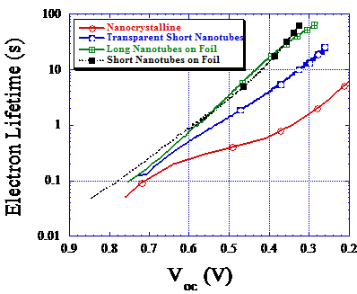
Above : Electron recombination lifetimes in dye-sensitized TiO2 nanotube arrays determined by open-circuit photovoltage decay. Electrons injected into the conduction band of anatase TiO2 nanotubes survive longer without recombining in comparison with nanoparticulate anatase electrodes. Consequently, nanotubes have improved charge collection efficiencies in dye-sensitized solar cells.

Forster Resonance Energy Transfer : The highly close-packed nanowire array architecture allows donor and acceptor dipoles to be within a Forster radius of each other. Therefore, electronic excitation energy can be efficiently transferred between donors and acceptors with sufficient spectral overlap. FRET is sensitive to the geometrical configuration of donors and acceptors. The inverse sixth power distance dependence of FRET only holds true for freely rotating dipoles. The distance dependence of FRET in the restricted geometry imposed by the close-packed NW arrays is unlikely to follow the inverse sixth power and is a subject of our studies.