2014
56. Piyush Kar, Samira Farsinezhad, Xiaojiang Zhang and Karthik Shankar, Anodic Cu2S and CuS Nanorod and Nanowall Arrays: Preparation, Properties and Application in CO2 Photoreduction, Nanoscale, 6, 14305-14318, 2014.

Abstract: Copper sulfide semiconductors made from earth-abundant elements have an optical absorption edge at ca. 1.2 eV, nearly ideal for solar energy harvesting. We report the growth and formation mechanism of vertically oriented arrays of copper sulfide nanostructures formed by electrochemical anodization. Key parameters that affect the morphology and phase of the nanostructures are type and strength of electrolyte, anodization voltage and duration. Cu2S and CuS nanostructures were obtained on both copper foil and copper-coated flexible Kapton substrates, and depending on the anodization parameters, consisted of vertically oriented arrays of nanowalls, nanoleafs or rods with branched nanodendrites. The anodization parameters also controlled the phase and stoichiometry of the nanostructures. p-type conduction for Cu2S nanostructures and n-type conduction for CuS nanostructures were revealed by admittance spectroscopy and Mott Schottky analysis. We also observed a weak, but nevertheless promising and previously unnoticed, photocatalytic action in copper sulfide nanorod and platelet arrays for the sunlight-driven conversion of CO2 into CH4. Under irradiation by AM 1.5G simulated sunlight at room temperature, a CH4 production rate as high as 38 μmol m−2 h−1 was obtained using the copper sulfide nanostructure arrays as stand-alone photocatalysts for CO2 photoreduction.
55. Farsinezhad S, Waghmare PR, Wiltshire BD, Sharma H, Amiri S, Mitra SK and Shankar K, Amphiphobic surfaces from functionalized TiO2 nanotube arrays, RSC Advances, 4, 33587-33598, 2014.

Abstract: Vertically-oriented, self-organized TiO2 nanotube arrays (TNAs) are a highly ordered n-type semiconducting nanoarchitecture with a wide range of potential applications. We generated low energy surfaces repellent to a broad spectrum of liquids by functionalizing TNAs using monolayers of two different fluorinated hydrocarbon molecules: perfluorononanoic acid (PFNA) and 1H, 1H′, 2H, 2H′-perfluorodecyl phosphonic acid (PFDPA). Nanotubes of two different outer diameters (50 nm and 130 nm) were studied and their wetting behavior analyzed in liquids belonging to different solvent classes to infer the nature of the wetting states. We show that the wetting behavior of perfluorinated monolayer-functionalized TNAs in polar liquids is explained by fakir or Cassie-states whilst the wetting behavior of bare nanotubes in every liquid is explained by Wenzel-type states. On the other hand, a transition between the Cassie and Wenzel states due to closed pores in the TNA architecture dictates the wetting behavior of functionalized TNAs in apolar liquids. The wetting behavior of functionalized TNAs is understood considering the synergistic effect of geometric and chemical surface modification. PFDPA-functionalized TNAs were found to be resilient to 24 hours of exposure to water and ethylene glycol at a static fluid pressure of 0.105 MPa, and are one step closer towards the realization of a mechanically robust omniphobic surface. At the same time, an understanding of wetting behavior will be useful in the design and optimization of a wide range of interface-sensitive devices such as metal oxide nanotube/nanopore array based sensors, implants, flow-through membranes, photocatalysts and heterojunction solar cells.
54. Mohammadpour A and Shankar K, Magnetic field-assisted electroless anodization: TiO2 nanotube growth on discontinuous, patterned Ti films, Journal of Materials Chemistry A, 2, 13810-13816, 2014.

Abstract: We present a magnetic field-assisted oxidation and etching process that transforms Ti thin films on arbitrary substrates into self-organized TiO2 nanotube arrays without the direct application of an anodization voltage between the cathode and the Ti film/substrate. In effect, the Ti film/substrate electrode is at a floating potential determined by the ionic Hall voltage. The development of such a magnetic field-assisted electroless anodization process, frees the anodization technique of forming nanostructured semiconductors and metal oxides from the constraints of substrate conductivity and film continuity imposed by the traditional anodization process, and allows the creation of uniform anodic nanostructures on pre-existing high-aspect ratio patterns as well as on substrates containing both conductive and non-conductive areas. Using magnetic field assisted electroless anodization, we demonstrate the formation of microscale patterns of high quality TiO2 nanotubes from discontinuous Ti films deposited on thermal oxide-coated Si substrates and patterned by a lift-off process.
53. Adl AH, Farsinezhad S, Ma A, Barlage DW and Shankar K, High performance ZnO TFTs through improved material processing and device design, The Proceedings of the ASME 2014 International Mechanical Engineering Congress & Exposition, Volume 2B: Advanced Manufacturing.
Abstract: Solution processing (SP) is a cheap, simple and high-throughput method for the fabrication of ZnO thin film transistors (TFTs). Lack of enhancement mode operation, poor crystallinity, traps, and poor control of the carrier concentration are some of the disadvantages of this method. The high intrinsic electron concentration of SP-ZnO makes saturation of TFTs non-trivial. We report on Schottky barrier thin film transistors (SB-TFT). By biasing the source Schottky contact in reverse bias, a depletion region is formed around the source contact hence depleting the region from the free charge carriers which produces the saturation of the device. The effect of the Schottky contact is illustrated by comparing the operation of SB-TFTs with that of conventional TFTs.
52. Farsinezhad S, Waghmare PR, Wiltshire BD, Amiri S, Mitra SK and Shankar K, The wetting behavior of TiO2 nanotube arrays with perfluorinated surface functionalization, The Proceedings of the ASME 2014 International Mechanical Engineering Congress & Exposition, Volume 9: Mechanics of Solids, Structures and Fluids.
Abstract: A facile electrochemical anodization method was used for producing hierarchically textured surfaces based on TiO2 nanotubes in two different configurations. It was found that perfluoro-functionalized TiO2nanotubes exhibit high static contact angles for a variety of liquids such as apolar, polar aprotic and polar protic solvents. Wenzel and Cassie-Baxter theories were applied for theoretical contact angle calculations for the present study. By using Cassie theories, it is shown that a drop of polar liquid was in a fakir or Cassie-Baxter (CB) state on perfluoro-functionalized nanotube surfaces. The fakir state prevents spreading of the liquid on the surface. On the other hand, the wetting of non-polar liquids such as hexane is characterized by either Wenzel states or transition states characterized by partial imbibition that lie in between the CB and Wenzel states.
51. Benlamri M, Bothe KM, Ma AM, Shoute G, Afshar A, Sharma H, Mohammadpour A, Gupta M, Cadien KC, Tsui YY, Shankar K and Barlage DW, High-mobility solution-processed zinc oxide thin films on silicon nitride, Physica Status Solidi - Rapid Research Letters, 8, 871-875, 2014.
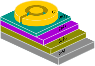
Abstract: A high effective electron mobility of 33 cm2 V–1 s–1 was achieved in solution-processed undoped zinc oxide (ZnO) thin films. The introduction of silicon nitride (Si3N4) as growth substrate resulted in a mobility improvement by a factor of 2.5 with respect to the commonly used silicon oxide (SiO2). The solution-processed ZnO thin films grown on Si3N4, prepared by low-pressure chemical vapor deposition, revealed bigger grain sizes, lower strain and better crystalline quality in comparison to the films grown on thermal SiO2. These results show that the nucleation and growth mechanisms of solution-processed films are substrate dependent and affect the final film structure accordingly. The substantial difference in electron mobilities suggests that, in addition to the grain morphology and crystalline structure effects, defect chemistry is a contributing factor that also depends on the particular substrate. In this respect, interface trap densities measured in high-κ HfO2/ZnO MOSCAPs were about ten times lower in those fabricated on Si3N4 substrates. (© 2014 WILEY-VCH Verlag GmbH &Co. KGaA, Weinheim)
50. He G, Delgado WT, Schatz DJ, Merten C, Mohammadpour A, Mayr L, Ferguson MJ, McDonald R, Brown A, Shankar K and Rivard E, Coaxing Solid State Phosphorescence from Tellurophenes, Angewandte Chemie, 53(18) 4587-4591, 2014.
Abstract: The synthesis of the first examples of tellurophenes exhibiting phosphorescence in the solid state and under ambient conditions (room temperature and in air) is reported. Each of these main-group-element-based emitters feature pinacolboronates (BPin) as ring-appended side groups. The nature of the luminescence observed was also investigated using computational methods.
49. Farsinezhad S, Dalrymple AN and Shankar K, Towards Single-Step Anodic Fabrication of Monodisperse TiO2 Nanotube Arrays on Non-Native Substrates, Physica Status Solidi A: Applications and Materials Science 211(5) 113-1121, 2014.
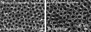
Abstract: Shape irregularity and size dispersion exhibited by TiO2 nanotube arrays (TNAs) is a disadvantage for size-selective applications such as flow-through membranes, cell differentiation and drug delivery, and for photonic applications such as photonic crystals and metallodielectric metamaterials, where size and shape dispersity are sources of defects and scattering. We show that achieving extremely smooth Ti films is more critical than a large Ti grain size in attaining highly ordered nanotube arrays with minimal dispersity in shape and size, and obtain the insight that uniform pore nucleation is determinative of the quality of the nanostructures that result following electrochemical anodization. TiO2nanotubes formed by anodization of highly smooth Ti films on single crystal silicon wafers in electrolytes with high water concentrations had only circular pores with a narrow dispersion of pore diameters, and exhibited uniform cross-sections along the tube-axis. Pattern order was evaluated using 2D-FFT analysis.
48. Mohammadpour A, Farsinezhad S, Wiltshire BD and Shankar K, Majority Carrier Transport in Single Crystal Rutile Nanowire Arrays, Physica Status Solidi - Rapid Research Letters (Special Issue: Focus on Functional Oxides) 8(6) 512-516 2014.

Abstract: Monocrystalline n-TiO2 nanowires of the rutile phase (Rtl-NWs) grown by a scalable hydrothermal method constitute a functional oxide nanomaterial with potential applications in photovoltaics, photocatalysts, field emitters and electrochemical battery anodes. Carrier transport in Rtl-NWs is of fundamental importance but has hitherto been inferred indirectly via impedance and intensity-modulated spectroscopic techniques. We report an effective electron drift mobility of 1.95 × 10⁻⁵ cm2 V–1 s–1 in rutile nanowire arrays directly measured using the time-of-flight (TOF) and space charge limited current techniques. In addition, we measure an equilibrium free electron concentration of ∼1014 cm–3 and a trap density of 3.5 × 1016 cm–3 in rutile nanowires. These results point to the importance of reducing traps to improve charge transport in rutile nanowires.