| Keypad Application Notes |
|---|
Introduction:
In this document, we will briefly discuss how to use the keypad. The keypad model is 4X4 series 83 which has 4 columns and 4 rows. We hope that our explanation and code will help other groups in the future.
Key Detecter:
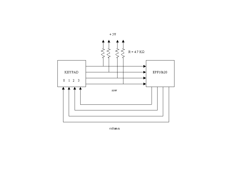
In our design, we use 4 columns as drive lines to drive 4 states into the keypad in order to detect which key is pressed. These 4 rows are sense lines to output the data into the FPGA. This diagram is shown below.
In our keypad decoder file, we define those columns as drive lines and rows as sense lines. Each of the 4-sense line is pulled up to voltage source with 4.7k ohm. So the original data for rows will be as high as "1111" without any keys being pressed. The drive lines drive 4 different 4 bit states. One bit will be low and the other three bits will be high impedance such as "0zzz" . Those 4 inputs will be "0zzz", "z0zz", "zz0z" and "zzz0". Once the sense lines sense a ‘0’, then we know that a key is pressed. The reason of ‘0’ appears is a line in the keypad is shorted to cause row bit value low. From the index number of column which has ‘0’ value and the index number of row which has ‘0’ value, we can detect which key is pressed according to our decoder file design. Then the key output data is sent out and the key will be released to continue operation. That is the way how keypad operates.
The following is the diagram (keypad.gif) about connection of the key and the FPGA chip.
Debouncing:
The most difficulty in the keypad decoder design is the debouncing. If the debouncing is not dealt properly, there would be no input into the keypad decoder and no output to FPGA. Then the keypad will not work. From my experience, the debouncing will take a time interval between 1ms to 10ms to settle down. So I pick 1ms for my debouncing period. Since the clock frequency I will use in the Altera EPF10k20 board is 25.175 MHz. In order to have 1ms delay, I use counter to count up to 25175 times. I am sure that signal will be stable enough after that period to send out.
Display:
The purpose of the displayer file is to display the keypad output on the Flex-digital display so that I have chance to figure out whether the right button is pressed from the display segment on the display. I can have 4-bit output from the keypad decoder and convert it into 7-bit output from the display file so that output can be displayed on the digital 7-segment display connected directly to the EPF10K20 device. Since I may have 15 different 4-bit output from the keypad decoder, I assign 15 different 7-bit output for converting.
Keytop:
The purpose of the keytop is to connect those 3 components together and work as one piece file so that I can run the whole file into the EPF10k20 chip to test the keypad. The input of keytop is the input of debouncing and the output is the output of displayer.
The following diagram (keytop.gif) is for the keytop:
