An automated video camera system is designed and implemented using a FLEX10K20 Altera FPGA. The FPGA controls the movement of the stepper motors by analyzing input signals from the video camera. The camera is part of a tracking system that detects the different light intensities between black and white. The white light will be targeted and followed in a complete 360o range of motion in the horizontal plane. This report describes the automated video camera system’s design approach, implementation and test cases to ensure functionality. Included in this report are hardware circuit schematic diagrams and connections, VHDL sub-component hierarchy & codes for the camera system with corresponding simulated testbench cases and overall FPGA logic space usage. Also included are the results of the testing after the final integration of the whole automated video camera system. Testing and modification of the VHDL code was done in both MaxPlusII and Mentor Graphics tools. In the end, all individual camera components are shown to be functional in both simulation and actual hardware testing, and are operating as designed in the original design proposal. The overall integrated system also performs to the specifications and exhibits all desired functionality.
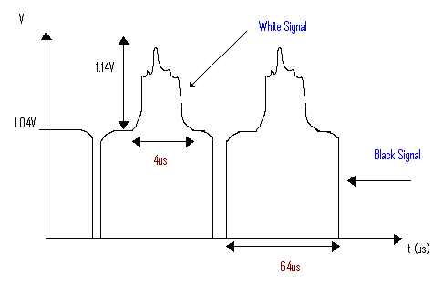
The video out signal will be taken from a NTSC video-out plug of a video camera. The voltage levels correspond to different colors of light that range from 0 to a slightly greater value than 1 volt. Voltage comparators will be used to distinguish the vertical and horizontal synchronous signals (deemed in this project to be between 0V and -0.5 V). The FPGA will count the number of clock cycles that the comparator signal is asserted low, and therefore the video signal is below the threshold. If the signal is low for the specified length of time (3.6us for a horizontal pulse, 1ms for a vertical pulse), a vertical or horizontal synchronous signal will be detected by the appropriate detector. If the signal is greater than or equal to 1V it can be classified as white light while 0V corresponds to the color black (see diagram below).
A ‘white light’ voltage comparator will compare a video out level to a reference voltage provided by the DAC08C (Digital Analog Converter) controlled from the FPGA with the video signal. For example, if the comparator detects “white” light for the majority of time in a vertical period (i.e. the comparator remains high between and for multiple pulses) then the FPGA will readjust the intensity level of the signal by decreasing the voltage level using the DAC threshold voltage. This will be done by coding the FPGA so that it sends an 8-bit feedback signal to the DAC. The DAC will shift the voltage threshold for the comparator downwards by a specified amount and therefore enable the system to detect different intensities in “white” light. However, if the video output signal is below the threshold voltage of the comparator (i.e. the comparator is remains low between pulses), the voltage threshold level must be shifted downward for it to detect white light.
Once the white light is detected by the FPGA, the stepper motors will reposition the camera accordingly to keep white light in the middle of the camera. Four output bits fed to horizontal stepper motor control the camera movement. The motor will move according to a set sequence of voltage pulses applied to the pins i.e. it will rotate left if pins 1,3,4&5 are pulses in that order. The FPGA will not be connected directly to the stepper motor instead driver chips will be used to provide the necessary power for the stepper motors. Since the stepper motor does not provide enough torque to move the test camera, a smaller and lighter camera is used. The motor’s speed will be uniform when moving in horizontal plane (360degrees). This simplifies the design and makes for easier VHDL coding.
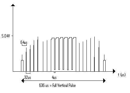
Every time a vertical pulse (see Figure 1b. for vertical pulse) is detected it signals the beginning of a new frame. Within two vertical pulses many horizontal pulses (see Figure 1c for Horizontal synch pulse) are to be found. If white light is encountered the relative distance between the horizontal pulse where the white light resides and the vertical pulse which signals the beginning of the frame, relates the direction of movement required for the camera. Two comparators will be used to detect the synchronous pulses, one for the horizontal pulses and one for the vertical pulses. The FPGA counts the number of clock cycles that the comparator’s outputs are asserted low to determine when the signal has been held below the threshold for the appropriate length of time. The horizontal pulses are approximately 3.6us in duration (at the horizontal comparator output) and the vertical pulses are approximately 1ms in duration (at the vertical comparator output). As a result, the FPGA can determine the type of synchronizing pulse as well as ‘count’ these pulses using a 9-bit counter. 9-bits are the required amount since there are 576 horizontal lines but since the video is scanned for even and odd horizontal lines simultaneously, there are only 255 horizontal synchs (see Figure 1d. for close-up view of Hsynch). The white sensitivity of the device will be controlled by the FPGA that will instruct the DAC to feed appropriate voltage signals to the voltage comparator that adjusts for different light intensities. The FPGA will need to temporarily store and compare the counts to align the camera properly using registers.

To control the stepper motor so that it detects and locks onto a white signal the following parameters are implemented in VHDL code:
Answer #1: The video camera signal are made of two main components, a vertical (Vsynch) and horizontal (Hsynch) synch. A vertical synch signals the start of the first scan line across a external video source, eg. TV. Within two Vsynchs there are approximately 576 Hsynchs (NTSC standard # of scan lines). The image information is carried in these Hsynch pulses as varying voltage values for different colors (see Fig. 1). The movement of the image is translated into horizontal voltage shifts on the Hsynch pulses. See diagram below.
To determine the y-coordinate, we simply need to count the number of Hsynchs pulses at any given time relative to a Vsynch pulse. The x-coordinate is determined by getting the time difference between an Hsynch and a white voltage signal. Since our video signal is analog, we will use voltage (LM311) comparators to output logic ‘1’ for Vsynchs & Hsynchs.
Answer #2: We are working with stepper motors and like all motors there is some back-EMF. We did not have the proper diode protection to our board because we only account for negative (VSS) back-emf. This was fixed by adding another diode to negate positive back-EMF. Also separate power supplies are used for the logic and motor drivers of the LS293D H-bridge chip with common ground. It helped with motor operation and it could save you $50 (cost to replace UP1 chip).
Answer #3: Overshoot occurs when the overcompensates for the location of a white object by turning too far in one direction. As a design decision, we decided to lower the stepper motor speed so that overshoot is minimized. This sacrifices response speed but increases the accuracy. It was also discovered that if the camera moved too quickly the motor would begin to oscillate because the object would appear on one side of the screen and then on the other causing the camera to turn back and forth.
Answer #4: Motor vibrations were dampened with a piece of styrofoam wedged between the mound and the platform. An inexpensive/low-tech solution that worked quite well. Another possible solution was to gear the motor; however, due to time and financial constraints this was not explored further.
Back to TopThe FPGA that will be used for this project is the Altera 10K20 + UP1. The board is chosen for its sufficient I/O pins, RAM and the number of logic cells for our project.
In the table shown below, are the pin assignments for the project components. The pin labels were found in the ‘flex10K_datasheet.pdf’ found on the EE552 website under “Local Copies of UofA Documentation”.
| Pin Label | Purpose |
|---|---|
| Dip 0 Switch #41 | Reset |
| 70 | Horizontal Synch Comparator |
| 62 | Vertical Synch Comparator |
| 67 | Comparator #2 Input (*White Light) |
| 64,66,68,71 | Output Pins to Stepper Motor |
| 45,48,50,53,55,61,63,65 | Output Pins to the DAC Unit |
| Algorithm | Logic Cells |
|---|---|
| Synch Control | 32 |
| Vertical Synch Detector | 47 |
| Horizontal Synch Detector | 21 |
| DAC | 15 |
| DAC Controller | 35 |
| Stepper | 47 |
| White Light Counter | 28 |
| Stepper Motor Controller (Shift) | 161 |
| Main | 386 |
| TOTAL | 386 |
Description: Added a module to the VHDL code to detect only 1 vertical synch pulse per full cycle, previous cases has been outputting multiple counts for each vertical synch pulse, since the video signal actually has multiple repetitions of the vertical synch pulse one right after the other for each cycle. A state machine (synch_control) was built to control the proper detection of the synch pulses. It waits for a vertical synch and then outputs a pulse, however it will not output another pulse until a horizontal synch is again detected.
Number of Logic Blocks: 16 Max. Freq.:29.95MHz
Conclusions/Results: The vertical synch pulses are now detected (in simulation) properly, although conflicts can arise between horizontal and vertical synch pulses as the vertical synch pulses can possibly be detected as a horizontal synch pulse initially before they are properly classified as vertical pulses.
Description: Changed the VHDL code for the synch controller element. The controller now detects a vertical synch pulse and then waits for a specified number of clock cycles to pass before it returns to a state which monitors the comparators for synch pulses. This prevents the detection of multiple vertical synch pulses during the series of pulses which follow the initial vertical synch pulse. This means that the state machine now has a counter to count the number of clock cycles and compares that number to the desired number to see if the appropriate length of time has passed yet. The addition of this counter added complexity to the synch controller module, and therefore reduced the maximum operating frequency below the 25.175 MHz that the FPGA is clocked at. A variety of experiments were performed in an attempt to increase the speed of the controller module.
The first few experiments concentrated on the comparison between the current count and the desired maximum count. The original comparison involved a < sign, by altering the code to allow the use of a <=,>,>=,/= (not equal), and = signs in the comparison. These changes did slightly affect the speed and size (in logic blocks) of the controller module.
| Comparison | Speed | Size (# of logic blocks) |
|---|---|---|
| < | 12.57 MHz | 28 |
| <= | 14.66 MHz | 29 |
| /= | 12.21 MHz | 30 |
| > | 12.46 MHz | 28 |
| >= | 14.73 MHz | 29 |
| = | 12.23 MHz | 30 |
None of these changes however increased the speed of the module to above 25 MHz. Therefore the counter, which was inside an if statement, which itself was inside a case statement inside the main process. First the code was altered so that the counter could be pulled outside the case statement. This decreased the complexity of the required logic and so the speed increased to 16.23 MHz. However the speed was still too low, therefore the counter was removed into a parallel process. This added a delay of one clock cycle to the output of the module, since the count needed to be registered to be accessible both by the main process and the counter process. However this latency is minor and the overall speed was increased to 46.72 MHz. After the overall size of the counter was increased to the needed size, the synch controller module still ran at 35.33 MHz, which is greater than the 25.175 MHz minimum required on the FPGA.
| Speed | Size (# of logic blocks) | |
|---|---|---|
| Original | 12.57 MHz | 28 |
| Counter outside case statement (but inside process) | 16.23 MHz | 21 |
| Parallel counter process | 46.72 MHz | 21 |
Description: Coded sequence for 4-wire stepper motor
Number of Logic Blocks: 8 Max. Freq.:125MHz
Conclusions/Results: Upon programming the FLEX10K20 chip and hooking up the stepper motor to the Expansion A pins the stepper motor did not turn. It was decided that the stepper motor did not react with the FPGA since the pulses may have been arriving too quickly for the stepper motor, therefore the delay time between pulses should probably be increased.
Description: Modified the VHDL code to include a delay of 1500 ns between each state assignment
Number of Logic Blocks: 8 Max. Freq.:125MHz
Conclusions/Results: Stepper motor reacted, but not as predicted. In the simulations, it was noted that the motor should turn and continue on turning provided that the input (pushbutton on UP1) was held down. In this case, the stepper motor would only turn briskly upon repeated pushing of the buttons (it was only being triggered on the push and the release). It was decided that a better solution may be to divide the clock pulses and to investigate into the stepper motor sequence again.
Description: Coded sequence for 4-wire stepper motor with clock division (2**23)
Number of Logic Blocks: 52 Max. Freq.:24.87MHz
Conclusions/Results: After a few technical difficulties (i.e. not connecting an output wire), the stepper motor functioned as predicted. When a pushbutton was held down, it turned in the appropriate direction and stopped as soon as soon as the pushbutton was let go.
Description: Coded sequence for 4-wire stepper motor with clock division (2**19)
Number of Logic Blocks: 43 Max. Freq.:27.24MHz
Conclusions/Results: As the number of clock divisions decrease, the stepper motor increased its angular velocity.
Description: The high moment of inertia of the camera/stepper motor structure caused significant vibrations every time the motor starts or stops. Therefore an acceleration/ deceleration unit was added to the stepper motor controller in an attempt to reduce physical vibrations and oscillations of the camera. The accelerator clock (pace at which clocks are switched) was started at 2**24.
Conclusions/Results: Acceleration may be too high, switch to slower clock
Description: Started Accelerator Clock (pace at which clocks are switched) at 2**28
Conclusions/Results: Acceleration is way too slow, took over 1 second to produce first step. Must change to slower clock 2**23 but change motor clocks
Description: Changed the four clocks to slower frequencies 2**24, 2**22, 2**20, 2**18
Conclusions/Results: Acceleration startup seems fine, with camera added the unit still oscillates therefore oscillation may not be dampened greatly by using acceleration/deceleration unit. Try physical dampening to remove the oscillations and vibrations instead.
Description: Sequence for DAC with Vref=1.0V increment/decrement by 1 (3.9mV)
Number of Logic Blocks: 29 Max. Freq. : 47.39MHz
Conclusions/Results: With the increment set to 1, each time the voltage is incremented it adds or subtracts 1/255 of the reference voltage, that would be 1/255*1V=0.0039V. This might prove to be too small of an increase, i.e. it may take too many clock cycles to increase the threshold. Try to increase by .025V which in turn is 0.025*255 ~= 7
Description: Sequence for DAC with Vref=1.0V increment/decrement by 7 (25mV)
Number of Logic Blocks: 29 Max. Freq. : 47.39MHz
Conclusions/Results: Increases and decrease voltage much more quickly. Have set a variable to allow for adjustment later on. No change in speed of FPGA with change of steps.
Description: Sequence for DAC with Vref=1.0V, Steps: 7, Latching Signals
Number of Logic Blocks: 31 Max. Freq. : 47.61MHz
Conclusions/Results: Done for the sake of testing it. No real loss in latching signals to clock. With the added ‘cost’ of 2 logic cells but a higher clock frequency, it may be good to keep it latched.
Description: Using a large white object to trigger the input “white_row_detected” the corresponding dac_up and dac_down signals were monitored.
Number of Logic Blocks: 21 Max. Freq. : 47.39MHz
Conclusions/Results: When the white object increased the number of white rows detected beyond the maximum value of 25, a “dac_up” signal ensued. When the number of white rows detected was less than 10 dac_down was enabled. Both inputs pulse as required but the “dac_down signal always follows a “dac_up” signal.
Description: Code was modified to account for the possibility of an input for “Vsynch” lasting longer than one clock cycle.
Number of Logic Blocks: 21 Max. Freq. : 47.39MHz
Conclusions/Results: The “dac_down” signal no longer follows the “dac_up” signal. The signal “dac_up” occurs to frequently due to the value of 25 for maximum white rows detected.
Description: Constants for maximum and minimum white rows detected were modified to 50 and 20 respectively.
Number of Logic Blocks: 21 Max. Freq. : 47.61MHz
Conclusions/Results: The “dac_down” and “dac_up” signals occur enough to give us enough selectivity for the threshold, but still trigger without reason. Could be that the “Vsynch” pulse is triggering when its not supposed to be.
Description: The code was changed to operate using a state machine to make the output signals more consistent with our expectations. Also, to eliminate any ambiguities caused by the “Vsynch” signal an internal clock is used instead to create a “Vsynch” pulse every 254 horizontal pulses.
Number of Logic Blocks: 51 Max. Freq. : 50.50 MHz
Conclusions/Results: Output signals are much are much more consistent than the previous code when its run using the “Hsynch” signal.
Description: Designed a module in VHDL to detect an output signal from the white light comparator and to output a logic ‘1’ whenever a target white light size (3 clock cycles) has been reached.
Number of Logic Blocks: 26 Max. Freq: 45.71 MHz
Conclusions/Results: As expected, the counter outputs a logic ‘1’ after 3 clock cycles. We did not refine the code or try other approaches because the maximum frequency is very acceptable (we need a minimum of 25.17 MHz which is the FPGA speed) and it worked properly. We verified this later using the oscilloscope.
All components were tested individually to ensure functionality in the fully integrated system and not just in individual simulations.
Back to TopDescription: To ensure that the FPGA correctly detects a vertical synchronous (v-synch) pulse from the video signal the v-synch signal was ported directly to an output pin and was compared to the video signal and the comparator output. The physical detection of the vertical synch pulse was not entirely reliable, i.e. the comparator output was not pulsing for every single cycle. In order to try to detect the signals more accurately all of the synch_detector and synch_controller parameters were tweaked. The two main parameters that were adjusted were the target pulse width (VSynchLength) and the vertical series delay factor (VseriesLength). The target width is the length of time that the comparator output goes low for when it detects a vertical synch pulse. It is entered in the number of clock cycles (at 25.175 MHz) that the detector has to count while the signal is low for the vsynch output to be pulsed. The series delay factor is an element that was built into the synch_controller module. It specifies a length of time after a vertical synch pulse is detected that the synch detector will ignore the input from the comparator so that multiple vertical synch pulses will not be detected in only one cycle. This is necessary due to the nature of the video signal.
Conclusions/Results: At first the code did not correctly output v-synch pulses when it was set to look for a target width of 500us per vertical pulse and a delay of 500us after each vertical synch pulse is detected. The v-synchs on the oscilloscope did not appear consistently at the correct v-synch times. Upon closer inspection of the signal, it is found that the target time needed to be decreased to 150us for correct v-synch detection. The major change in this parameter was due to a change in the voltage of the comparator power supplies since the first measurements. It was also found that the vertical series delay could be lowered to 363 us while maintaining proper functionality. Upon using these values, the FPGA outputs a correct pulse at each V-synch signal, but is still not entirely consistent
Description: Another comparator circuit was built to exclusively detect the vertical synch pulses. This comparator’s reference was to ground instead of the other synch comparators reference to slightly negative value. The separate comparator allowed more accurate detection of vertical synch pulses.
Conclusions/Results: After the additional comparator circuit was hooked up it was used to send signals to the FPGA regarding the vertical synch pulses. Due to the adjusted threshold changes a 1ms pulse is now the target. This is far easier for the detector to accurately find. Now that both the vertical and horizontal synch pulse detectors each had their own comparator they were detected reliably and the FPGA output showed the desired functionality.
Description: To test if the FPGA outputs a pulse whenever the camera
detects the color white. The camera was hooked up to the FPGA and the oscilloscope
was used to monitor the white signal comparator line and the FPGA output. Different
sizes of white objects were used at various distances and light intensities.
Conclusions/Results: The detection process behaved as expected from the
simulations. The white light pulses from the FPGA shifts with the movement of
the color white. See the report for clarifications.
An error occurs when the color white covers more than 80% of the camera image area. The signal seen on the oscilloscope shows a ‘black’ signal rather than the expected ‘white’ signal. We suspect that the white light comparator chip is sensitive to light levels (i.e. shadows cast on the camera as objects get closer). Since it only detects two thresholds, it cannot detect anything in between. Therefore, the slightest change in lighting will cause the comparator to output a black signal. This problem is not a serious issue since the DAC controller will compensate for this error through automatic threshold adjustments.
Back to TopDescription: Horizontal Synchs output from the FPGA was taken from an I/O pin and measured directly using the lab’s oscilloscope. We expected to see many spikes that correlates to the Hsynch pulses. Since it is impossible to observe all 255 horizontal pulses on the oscilloscope, we decided to take a time average of the horizontal pulses within ~3.3ms. We expect to see around 50 horizontal pulses.
Math:
Vertical Refresh rate: 1/60s
Number Horizontal Scan Lines: 255
Time per scan line = (1/60s)/255lines = 65.34us/line
Desired # of scan lines = 65.34us/lines x 50lines (horz. pulses) = ~ 3.3ms time frame
There we set a time frame of 3.3ms and counted roughly 40 horizontal pulses.
Conclusion/Results: Although we only counted 40 horizontal pulses, this is an acceptable value since we are not looking specifically at an exact number of pulses but rather an average of Hsynch pulses. We could actually control the number of Hsynch pulses that we see by changing the pulse width time that we are looking for in the VHDL code. By decreasing the time interval for each pulse from 5us to 3.2us, the number of horizontal pulses should increase. This was verified on the oscillscope.
Description: We compared the number of Hsynch’ seen to the actual video signal that was fed into the comparator. Increasing the time frame to the micro-second range, we are able to determine the number of Hsynch pulses seen from the FPGA match the number of Hsynch from the video signal.
Conclusion/Results: By direct visual inspection, we find that a scan time of 3.2us for each horizontal synch is acceptable in production enough Hsynch pulses. It is determined that actual measurements made to determine Hsynch pulses are not accurate time values in the detection process.
Description: The experiment for the stepper motor control is determined by two push buttons on the FPGA. Push button 1 (PB1) would control the clockwise rotation and push button2 (PB2) controls the counter- clockwise rotation.
Conclusion/Results: The motor turned properly in response the correct pushbuttons. It is concluded that proper stepper motor movement can be controlled.
Description: The experiment for the stepper motor torque is tested.
Varying supply voltage values in the range of 5->15V, the torque is tested using
a sophisticated process of holding the motor axis and seeing if it can be physically
moved.
Conclusion/Results: At 15V, the motor torque is at its greatest. However
since we are keeping all supply voltages to +/- 5V, it is determined that at
5V the motor torque is acceptable to rotate a camera. Also adjusting FPGA clock
time between motor pulses from a rotation stage to the next could also vary
motor torque. The optimum clock time is determined to be: (2^21)-1.
Back to Top
Description: Initially, the shift code determines the left and right movement of the stepper motor. As a debugging process, the left and right signals are assigned output pins at the FPGA to test the left and right movement of the shift code at the same time testing the movement of the stepper motor.
Conclusions/Results: The left and right output pins of the FPGA will clearly show the correct or wrong rotation of the camera.
Initially, the camera will not move along with a test white object. Hence, it was found out that the code did not take into terms undefined range of time. The left and right output signal of the shift code was undefined during undefined times. The shift code was revised with a reset state to initialize the left and right signal to ‘low’. Hence, reset must be set for every test run.
Moreover, it was found that the left signal was always pulsing even though the test white object was placed at the right side of the camera’s sight range. However, there were more right pulses showing in the oscilloscope than left pulses. Hence, an averaging design was implemented to the code. The averaging design basically counts the number of left and right pulses individually. The overall code will output the signal with the highest pulse count after a certain number of vertical synchs and drive the motor left or right at that moment in time.
Furthermore, it was found out that an object’s center mark couldn’t be treated as a point. If it was treated as a point the camera and/or motor will overshoot it. The overshoot is due to the motor’s own mechanical overshoot while rotating and then changing direction. Hence, a safety range is implemented to the code. The center mark is change from a point to a range of points. The range was modified many times until the correct rotation of the camera was achieved. Furthermore, a simple Styrofoam dampener was placed at the bottom of the camera to further reduce the mechanical overshoot.
Number of Logic Blocks: before 59 and after revision 1.61
Max. Freq.: before 40.16 MHz and after revision 57.47 MHz
In conclusion, the modification to the code required more logic cells and was a bit slower. However, our project was able to tolerate the increased logic usage and slower speed.
Description: Testing the functionality of the DAC_CONTROL consisted of using the input from the white comparator and observing the corresponding outputs for “dac_up” and “dac_down” signals on the oscilloscope. In order to activate the required output signals a white object was placed in front of the camera. As the white object was moved within and outside the cameras visual range the white input signal from the comparator varied above the maximum threshold set to 50 and below the minimum of 10.
Conclusions/Results: In order to satisfy the minimum value of white rows detected the camera basically had to be focused upon a black object due to the white light noise in the surrounding environment. Between the ranges of maximum and minimum the output signals appeared to be set low as expected. If the white object was placed on the outer edges of the camera the dac_up signal was set high increasing the threshold. This operation makes sense given that when the white object is detected on the outer edges of the camera, it is repositioned by the stepper motor bringing the white object closer to the center. The increase in the threshold directly compensates for the fact that the object will occupy a larger part of the video signal.
Description: We tested to see if the entire design would function properly. A black background was put in front of the camera to see if it would not move when there was no white object present. The camera was also turned off to test for the lack of synch signals.
Conclusions/Results: As expected, it did not move/rotate indicating that the camera operates properly when no white light was detected or when the camera was turned off.
Description: A white strip is introduced into against the black background to see if it will move left or right based on white light movement.
Conclusions/Results: It could rotate right but had a hard time moving left. The safety margin in the ‘shift.vhd’ code was increased. This gave better results since it now moved left and right. The area of the white object is an essential factor in camera movement and needs to be considered in the camera optimum range of operation.
Description: Tested the camera under different lighting levels from black to a fully lit room.
Conclusions/Results: The camera has trouble operating in a fully lit room since there are light reflections and glare off of various objects (even black surfaces). It follows a light source very well in a darkened room. The DAC needs tweaking since it controls the white light threshold level. Ideally, we want it to be able to operate in a wide range of lighting conditions.
Description: Tested to see if the camera would follow a flashlight in low lighting conditions at a distance of 3’.
Conclusions/Results: The camera successfully tracked the flashlight.
Description: Tested to see if the camera would follow an 8’x 11’ piece of paper against a black background at a distance of 6’.
Conclusions/Results: The camera successfully tracked the paper, although it sometimes got very confused (or lock in a position) if it caught a reflection of light from a window or computer monitor.
Description: Tested to see if the camera would follow a person wearing an 10cm x 10cm piece of white paper in low lighting conditions at a distance of 6’.
Conclusions/Results: The camera successfully tracked the person through 360o when they moved at a reasonable pace. If the person moved too fast and the camera lost track of the person, the camera would successfully relock onto them when they came back into the camera’s field of view.
Description: Tested to see if the camera would follow a person wearing an 10cm x 10cm piece of white paper in mid-lighting conditions at a distance of 6’.
Conclusions/Results: The camera successfully tracked the person through 360o when they moved at a reasonable pace. This is the final test that is performed on the design. There is no time left for any improvements, however we have met our goal of successful automated tracking of white light in the horizontal plane.