Viterbi Decoding for Convolutional Codes is presented here as an efficient system for reliable communication over noisy digital communication channels. However, traditional implementation of Viterbi decoding using software cannot keep up with the speed requirements for digital data transmission. An alternative is to use Field Programmable Gate Array(FPGA) implementation at which higher speed can be achieved.
This project considers the problem of designing a system which implements Viterbi Decoder for Convolutional Coded signals using FPGA. This system is divided into two distinct part: the Decoder System and the Test System. The decoder system implements the Viterbi Algorithm for decoding soft decision inputs. The test system functions as an off-line testability and employs an on-chip circuitry as part of the decoder design to accomplish testing and make decoding circuits easily testable. To achieve this, the test system utilizes the Convolutional Code Encoder as part of the system. Very High Description Language(VHDL) is used for the whole system design.
Due to the need to physical Random Access Memory(RAM), the system design is build on the Rapid Prototyping Board(RPB) using two Xilinx 4000 Series FPGA’s. Design Architect is used for coding VHDL and Quicksim is used for simulation and design verification. VHDL codes are synthesized into FPGA using Synopsys Synthesis tools. The constraint length 5 with code rate ½ are considered here for both decoder system and test system.
Table of Contents
List of Tables and Figures
Our design is implemented in 2 Xilinx 4010 FPGA chips. Metric and survival calculation is implemented in FPGA2, while the rest of the design is implemented in FPGA1. A total of 1026 CLBs (Configurable Logic Blocks) are used. The input-output pin assignment is shown in the following tables.
FPGA1:
System input-output using proto connector A of FPGA1, and is shown in the following table.
Table 1: FPGA1 and Corresponding Pin assignments
| FPGA1 Pin Name | FPGA1 Pin Number | In/Out | VHDL In/Out Name | Function |
|
V5 |
Connect to Switch 1 |
In |
Reset |
System Reset, |
|
U1 |
In |
MaxClk |
Input Clock to System | |
|
V15 |
40 |
Out |
SysClk |
System clock generated from MaxClk |
|
U14 |
39 |
In |
BvDataIn1(2) |
Bit 2 of Data1 for Branch Metric calculation |
|
T13 |
38 |
In |
BvDataIn1(1) |
Bit 1 of Data1 for Branch Metric calculation |
|
V16 |
37 |
In |
BvDataIn1(0) |
Bit 0 of Data1 for Branch Metric calculation |
|
U15 |
36 |
In |
bvDataIn0(2) |
Bit 2 of Data0 for Branch Metric calculation |
|
T14 |
35 |
In |
bvDataIn0(1) |
Bit 1 of Data0 for Branch Metric calculation |
|
U18 |
34 |
In |
bvDataIn0(0) |
Bit 0 of Data0 for Branch Metric calculation |
|
J17 |
5 |
In |
bEncoderIn |
Data Input to Encoder |
|
J18 |
4 |
In |
Mode |
Mode selection |
|
H18 |
3 |
Out |
mSequenceOut |
Data Out from m-Sequence unit |
|
H17 |
2 |
Out |
bDecodeOut |
Decoder Output |
|
H16 |
1 |
Out |
bEncoderOut |
Encoder output |
Communication between FPGA1 and FPGA2 using hard-wired pins specified in RPB (Rapid Prototyping Board ), and is shown in the following table.
Table 2: FPGA1 and FPGA2 and the Corresponding Functions
|
FPGA 2 |
FPGA 1 |
VHDL In/Out Name |
Function |
||
|
PIN Name |
In/Out |
PIN Name |
In/Out |
||
|
C2 |
Out |
V2 |
In |
bvSurvival(15) |
Calculated survivals, bit 15 |
|
A3 |
Out |
U2 |
In |
bvSurvival(14) |
Calculated survivals, bit 14 |
|
A7 |
Out |
V7 |
In |
bvSurvival(13) |
Calculated survivals, bit 13 |
|
A4 |
Out |
V4 |
In |
bvSurvival(12) |
Calculated survivals, bit 12 |
|
A5 |
Out |
V5 |
In |
bvSurvival(11) |
Calculated survivals, bit 11 |
|
A6 |
Out |
V6 |
In |
bvSurvival(10) |
Calculated survivals, bit 10 |
|
A7 |
Out |
V7 |
In |
bvSurvival(9) |
Calculated survivals, bit 9 |
|
A8 |
Out |
V8 |
In |
bvSurvival(8) |
Calculated survivals, bit 8 |
|
A9 |
Out |
V9 |
In |
bvSurvival(7) |
Calculated survivals, bit 7 |
|
A10 |
Out |
V10 |
In |
bvSurvival(6) |
Calculated survivals, bit 6 |
|
A11 |
Out |
V11 |
In |
bvSurvival(5) |
Calculated survivals, bit 5 |
|
A13 |
Out |
V13 |
In |
bvSurvival(4) |
Calculated survivals, bit 4 |
|
A14 |
Out |
V14 |
In |
bvSurvival(3) |
Calculated survivals, bit 3 |
|
A12 |
Out |
V12 |
In |
bvSurvival(2) |
Calculated survivals, bit 2 |
|
A17 |
Out |
V17 |
In |
bvSurvival(1) |
Calculated survivals, bit 1 |
|
C4 |
Out |
U4 |
In |
bvSurvival(0) |
Calculated survivals, bit 0 |
|
B5 |
In |
SysClk |
System Clock | ||
|
B6 |
In |
bvDataIn1(2) |
Bit 2 of Data1 for Branch Metric calculation | ||
|
B9 |
In |
bvDataIn1(1) |
Bit 1 of Data1 for Branch Metric calculation | ||
|
B10 |
In |
bvDataIn1(0) |
Bit 0 of Data1 for Branch Metric calculation | ||
|
B11 |
In |
bvDataIn0(2) |
Bit 2 of Data0 for Branch Metric calculation | ||
|
B12 |
In |
bvDataIn0(1) |
Bit 1 of Data0 for Branch Metric calculation | ||
|
B13 |
In |
bvDataIn0(0) |
Bit 0 of Data0 for Branch Metric calculation | ||
The satellite and space communication channels are likely candidates for the cost-effective use of coding to improve communication efficiency. The primary addictive disturbance on these channels can usually be accurately modeled by Gaussian noise which is ‘white’ enough to be essentially independent from one bit time interval to the next. Not particularly on the space channel but also in many instances on satellite channels, sufficient bandwidth is available to permit moderate bandwidth expansion. The effective decoding algorithms for independent noise (memoryless) channels have been developed and refined, namely Viterbi Decoding for Convolutional Codes. Combined with real communication needs and the availability of digital integrated circuits such as Field Programmable Gate Arrays(FPGA), practical and powerful high speed decoders for communications over noisy channels are now possible.
The design of Viterbi Decoder for Convolutional Coded Signals system using FPGA’s is divided into two subsystems, namely the decoder system and the test system. The decoder system, which is the Viterbi decoder, implements the Viterbi Algorithm. Viterbi Algorithm is a recursive optimal solution to the problem estimating the state sequence of a discrete time finite-state Markov process observed in memoryless noise. The test system functions as an off-line testability with minimum sharing of decoder resources. This employs an on-chip circuitry as part of the decoder design to accomplish testing and make decoding circuits easily testable. The test system implements the convolutional code signals to test the decoder system which is generated by the convolutional code encoder.
Hence, the chip generated in this project functions as a decoder, specifically Viterbi decoder, for digital communications over noisy channels. Occasionally, this chip can be easily self-tested to make sure the decoder is still functioning properly. In addition, this chip does have another function, that is to function as a convolutional code encoder.
In designing the whole system, the targeted specification for both the decoder system and the test system are set as follows:
Figure 2.1.1 shows the general system block diagram for this project. The Decoder System consists of the Decoder itself and the Test System consists of the M-Sequence Generator, the Encoder System and the Serial-Parallel Converter.
The mode for this system is controlled by the input MODE. At MODE ‘1’, which is the Decoder Mode, the M-Sequence Generator, the Encoder System and the Serial-Parallel Converter are disabled. Hence, only the Decoder System are enabled. At this mode, the decoder accepts ‘soft decision’ inputs from the 6-bit Decoder Input. The Decoder will then decodes the received data and transmits the decoded data at the Decoder Output.
However, at MODE ‘0’, which is the test mode, the Decoder accepts input from the output of the Serial-Parallel Converter. At this mode, the M-Sequence Generator, Encoder System and the Serial-Parallel Converter are enabled. The M-Sequence Generator generates random test pattern for M=3. The Encoder System will then encodes the random test patterns and the Serial-Parallel Converter will simulate a 6-bit ‘soft decision’ output for the corresponding convolutional encoded test pattern. The Decoder will then decode the simulated output and transmit results at the Decoder Output. A comparison can then be made by comparing the bits obtained from the Decoder Output and the M-Sequence Generator. The Encoder System can be configured independently. This means that the encoder accepts data from the Encoder Input, and transmits the results at the Encoder Output.
The overall design is carried out using VHDL code. Modular design is used. Total 5 hierarchy levels are used. The design hierarchy for the whole system is shown as below:

A binary convolutional code rate , r, of ½ bits/symbol is generated by a linear finite state machine consisting of a 5 stage shift register(K=5), 2 modulo-2 adders connected to some of the shift register stages, and multiplexer that scans the output of the modulo-2 adders. This is the essence of the encoder system which is shown in block diagram in Figure 2.2.1.

The shift register is initially filled with an all zero sequence and the first binary digit(referring to Figure 2.2.1, the first binary digit is ‘1’) is fed into the first stage of the register. The modulo 2 adders are then sampled in sequence by the multiplexer, producing 2 output coded symbols(‘11’) which are then transmitted into the channel.
After the first 2 coded symbols are obtained, the second input ‘1’ is shifted into the first stage of the shift register, causing the contents of all the other stages to move one step to the right. The rightmost digit leaving the encoder is lost. The 2 modulo 2 adders are sampled again, yielding 2 new output symbols, ‘01’ which are again transmitted. This procedure continues until the last input digit, for the case in Figure 1.1, ‘0’ enters the shift registers, yielding 2 symbol output ‘00’.
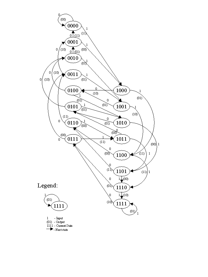
The above procedure can be viewed in a finite state machine with transition from the old state to the new state for a given binary input will yield 2 output coded symbols. The state of the system is given by the first 4 stages of the shift registers and the last stage of the shift registers is omitted as it will be lost during the transition. The state table and the state diagram for this encoder system are shown in Appendix A1 and Appendix A2 respectively.
Translating block diagram in Figure 2.2.1 into schematic level, a system with 4 D-Flip-flops, 2 Modulo-2 adders and a 2-1 multiplexer is obtained as shown in Figure 2.2.2 below.

The MODE input controls the whole encoder system, that is if MODE=’0’, the encoder system is enabled and otherwise for MODE=’1’. Bit_in is the binary input shifted into the flip-flops at each clock/2. RESET input resets the whole system. Notice that the clock input to the flip-flops is CLOCK/2 and the clock to the multiplexer is CLOCK. This is due each binary input symbol to the registers will generate 2 coded symbols at the output. Thus, a clock divider is inserted at the input to the encoder system.
2.3.1VHDL implementation of the Encoder System
The encoder system is an essential part of the test system in which will be discussed later. Here, VHDL is used throughout the whole system as well as this project. Figure 2.2.3 shows the hierarchical level of the encoder system in VHDL used in this project.

In Figure 2.2.3, entity clock_divide divides the clock input to half of the clock input. Entity encoder is a top level entity for entity shiftadd and mux21. Entity shiftadd functions as the shift registers and the modulo-2 adders and entity mux21 is the multiplexer of the encoder system. The VHDL codes for the encoder system is shown in Appendix A3 as part of the Test System.
The decoder system is the kernal of our project. We implement Viterbi algorithm in decoder to decode convolutional codes. Our design choose constraint length K = 5, trellis truncation depth L = 20, and rate R= ½. The Viterbi decoder is consisted of 4 sub-units: Branch Metric( BM ) Unit, Add-Compare-Selection( ACS ) Unit, Memory, and Output Unit. The data flow among units are shown below :
![]()
We will discuss the design of each unit in the following sections.
First, We give a brief introduction about Viterbi algorithm. Viterbi algorithm is a special case of Bellman Ford shortest distance algorithm. We illustrate the basic concepts involved by a simple K = 3 convolutional code. Trellis is defined as state diagram with time stamp, i.e., timed state diagram. The trellis and the state diagram of K = 3 convolutional code is shown Figure 2.3.1.

A Branch is defined as one step state transition. A Path is defined as a sequence of state transitions with corresponding input and output data. A Stage is defined as all states at one time stamp. Metric is defined as distance between two code words or code sequences. We use absolute difference as metric.
Path metric PMi,j at state i of stage j is calculated from branch metric BMh,i as :
![]()
Viterbi Algorithm select the sequence on trellis that has smallest distance with the received data sequence as decoded sequence. Selection is proceeded stage by stage. If state h of stage j-1 store minimum path metric PMh,j-1 , then the minimum path metric PMi,j at state i of stage j is :
![]()
The selected branch is called Survival. The selected path metric is called Survival Path Metric.
Our main task is to implement the above algorithm in FPGA. We use BM unit to calculate branch metric. We use ACS unit to calculate path metric and survival. The survivals are passed to memory unit, which will carry out traceback decoding. The output from memory unit is in reverse-order of the received bit stream, so we use a special output unit to generate the decoded bit stream in correct order.
2.3.2 Branch Metric( BM ) Unit
The BM unit is used to calculate branch metric for all 16 trellis branches from the input data. We choose absolute difference as measure for branch metric, which can be implemented as adders as shown in the following BM unit diagram.

Here, bvDataIn0 and bvDataIn1 is 3-bit input data to BM unit after A/D and Serial/Parallel conversion from received channel output, while bvBranchMetric0 - bvBranchMetric3 is the calculated branch metric.
BM unit is implemented in entity BranchMetric.
2.3.3 Add-Compare-Selection( ACS ) Unit
The ACS unit is used to calculate the path metrics for each state in current stage from path metrics of its 2 previous states and the associated state-transition branch metric, then the path with least path metric is selected as survival path for the state in current stage. The survival is encoded as 1 bit, which is stored into memory. An 8 bit adder is used for path metric calculation. The survival selection is implemented by 8 bit subtraction, the path metric of the survival is stored in 8 bit register inside ACS unit.
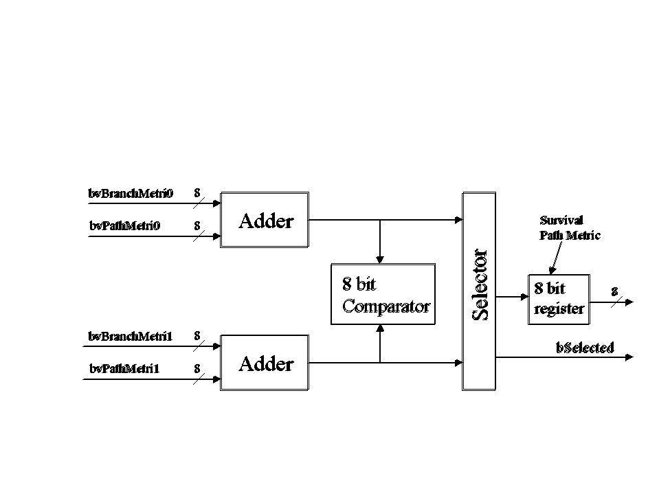 Figure
2.3.3: Add-Select-Compare Unit
Figure
2.3.3: Add-Select-Compare Unit ACS unit is implemented in entity ACS.
We generate decoded data from calculated survival in ACS using traceback scheme. It’s based on the following important property of trellis :
All survival paths start from current stage j will merge at stages £ j - 4K.
Traceback is carried out in memory unit. Memory unit have the following implementation details:
A. Generate decoded data by traceback reading the survival path for 4K stages.
B. Survival is stored in memory (SRAM in Xilinx chip). Memory is organized as 6 16x10 memory banks.
C. Each memory bank has 6 states: Write (WR ), Decode read ( DC ), Idle, Traceback read 1 ( TB1 ), Idle, Traceback read 2 (TB2).
D. Decoded data (Traceback Out ) is generated in decode read. It’s in reverse order of input data.
The schematic diagram for memory unit and state diagram for memory bank is shown as below.

The memory unit is implemented in entity MemSys.
It’s used to generate decoded data stream in correct order from the reverse-ordered traceback output. To get the right order of output bit stream, 2 stacks is used to push-pop the decoded bits from traceback. Each stack will be run in pop mode or push mode in turn. The 2 stacks are always in different mode. Each stack is implemented using SRAM in Xilinx chip. The schematic diagram for output unit is shown as below.

Output unit is implemented in entity SysOut.
As stated in the design objective, a test system is implemented. The test system functions as an off-line testability with minimum sharing of decoder resources. This employs an on-chip circuitry as part of the decoder design to accomplish testing and make decoding circuits easily testable. The test system implements the convolutional code signals to test the decoder system. In addition, it contains several other testing circuits to accomplish complete testability on the decoder system.
The test system uses the encoder system(as described earlier) as part of the design to accomplish its objectives as stated above, which is to use convolutional coded signals to test the decoder system. In addition, it uses several other components such as the M-Sequence Generator and the Serial-Parallel Converter to accomplish the task of simulating a ‘soft decision’ output to the decoder for testing. The block diagram for this test system is shown previously in Figure 2.1.1 of the system block diagram.
The M-Sequence Generator generates a sequence of random test data for M=3. The M-Sequence Generator will need the clock input for the period of each test bit and the MODE input. The Serial-Parallel Converter converts the encoded test pattern and simulates a 6-bit ‘soft decision’ output for the decoder system. For simplicity for this project and to be consistent with the decoder system design, the output of the Serial-Parallel Converter is such that the first 3 bits are the most significant bit(MSB) of the 2-bit encoded symbols from the encoder system and the latter 3 bits are the least significant bit(LSB).
2.4.1 VHDL implementation of the Test System
Figure 2.4.1 shows the hierarchical level of the test system in VHDL used in this project.

Entity generator is the M-Sequence Generator and entity serial_parallel is the Serial Parallel Converter. Here in the figure, the pin time2SysClk is the system clock, bvDataOut0(2 downto 0) and bvDataOut1(2 downto 0) are both 6-bit simulated ‘soft decision’ output to the decoder system and bdataOut is the encoded symbols from the encoder system. The VHDL codes for the test system is shown in Appendix A3.
This section describes the simulation done for the test system and the decoder system. Here, the design tool, QuickSim, is used for the simulation.
The test system in Figure 2.4.1 is simulated using the test file shown in Appendix A3. The simulated output timing waveform is shown in Figure 3.1.1. For the purpose of describing the timing waveform, only selected signals of the system are shown in Figure 3.1.1.
Referring to the timing waveform, from time 0-50ns, the mode input is ‘1’. At this mode, the test system is disabled. Here, the output bvdataout0, bvdataout1 and bdataout are in high impedence state.
However at time 100ns, the mode is ‘0’ which enabled the test system. The reset at 100ns resets both bvdataout0 and bvdataout1 to ‘000’ and ‘000’ respectively. After the reset, the M-Sequence Generator start to generate test data at the generator ‘bit_out’. The 5 test bits generated for this case are ‘11001’. The state of each shift registers in entity shiftadd are shown by the signal q. Here, the shift registers shift to the right for each input. The rightmost digit leaving the 5-stage register is lost.
By referring to the state table for convolutional code encoder, each state transition for the input test bit ‘11001’ will generate output symbols of ‘11’,’01’,’00’,’11’ and ‘01’ respectively. These output symbols will be converted by the Serial-Parallel Converter to simulate a soft decision for the decoder system. For this case, The LSB of each generated symbol is given by bdataout0 and MSB is given by bdataout1. Observing bvdataout0 and bvdataout1 in Figure 2.4.1, the corresponding results are ‘111’, ‘111’, ‘000’, ‘111’, ‘111’ for bvdataout0 and ‘111’, ‘000’, ‘000’, ‘111’, ‘000’ for bvdataout1. Thus, the results here verified that the test system works as expected.
The operation of Viterbi decoder is simulated under Mentor Graphics. We show the selected traces in the next two pages, Figure 3.2.1 and Figure 3.2.2. In the traces, Sysclk is the clock for decoding input data stream, which is the rate of generating decoded data. Reset0 is system reset. bDecodeOut is the decoded output data stream from decoder. bDataIn is the output of m-Sequence generator, which is also the input to convolutional code encoder. bvSurvival, vPathMetric(15) and vBranchMetric(3) are the calculated 16 bit survivals, path metric of state 15 and one of branch metric from metric calculation. Current state is the state of memory bank #5. PopDataOut is the output from stack0. After some latency, Decoder output ( bDecodeOut ) is generated nicely, which can be compared with the output from m-Sequence generator ( bDataIn ).
An approach has been made in this project to implement Viterbi Decoder for Convolutional Coded Signals using FPGA. VHDL is used for the whole design. This approach has yet to be successful. The design of the decoder system has proved to be very complicated due to its nature of complexity and time constraint. The constraint length K used for both the decoder and test system is 5. At this constraint length, with a code rate of 1/2, the trellis truncation depth has to be at least 20. Thus, this will require a significant amount of RAM and a good memory management using VHDL is essential.
However, the test system worked as proposed for this project and has been successfully demonstrated. The test system employs the M-Seqence Generator, the Encoder System and the Serial-Parallel Converter. Using these three primary components, the test system had been successful to simulate a 'soft decision' test data for the decoder input.
This project has proved to be a positive learning experience both for an engineering profession and to design a considerably complicated system. Here, we had learned to use VHDL to develop applications using FPGA. In addition, we had learn several useful CAD tools during the course of the project such as Mentor Graphic's Design Architect, QuickSim, Actmap, Synopsys Synthesis Tools and using the Rapid Prototyping Board to implement hardware applications.
STATE TABLE FOR CONVOLUTIONAL CODE ENCODER
|
Old State |
Input |
New State |
Output |
|||||||
|
0 |
0 |
0 |
0 |
0 |
0 |
0 |
0 |
0 |
0 |
0 |
|
0 |
0 |
0 |
0 |
1 |
1 |
0 |
0 |
0 |
1 |
1 |
|
0 |
0 |
0 |
1 |
0 |
0 |
0 |
0 |
0 |
1 |
1 |
|
0 |
0 |
0 |
1 |
1 |
1 |
0 |
0 |
0 |
0 |
0 |
|
0 |
0 |
1 |
0 |
0 |
0 |
0 |
0 |
1 |
0 |
1 |
|
0 |
0 |
1 |
0 |
1 |
1 |
0 |
0 |
1 |
1 |
0 |
|
0 |
0 |
1 |
1 |
0 |
0 |
0 |
0 |
1 |
1 |
0 |
|
0 |
0 |
1 |
1 |
1 |
1 |
0 |
0 |
1 |
0 |
1 |
|
0 |
1 |
0 |
0 |
0 |
0 |
0 |
1 |
0 |
1 |
0 |
|
0 |
1 |
0 |
0 |
1 |
1 |
0 |
1 |
0 |
0 |
1 |
|
0 |
1 |
0 |
1 |
0 |
0 |
0 |
1 |
0 |
1 |
0 |
|
0 |
1 |
0 |
1 |
1 |
1 |
0 |
1 |
0 |
0 |
1 |
|
0 |
1 |
1 |
0 |
0 |
0 |
0 |
1 |
1 |
1 |
1 |
|
0 |
1 |
1 |
0 |
1 |
1 |
0 |
1 |
1 |
0 |
0 |
|
0 |
1 |
1 |
1 |
0 |
0 |
0 |
1 |
1 |
0 |
0 |
|
0 |
1 |
1 |
1 |
1 |
1 |
0 |
1 |
1 |
1 |
1 |
|
1 |
0 |
0 |
0 |
0 |
0 |
1 |
0 |
0 |
1 |
0 |
|
1 |
0 |
0 |
0 |
1 |
1 |
1 |
0 |
0 |
0 |
1 |
|
1 |
0 |
0 |
1 |
0 |
0 |
1 |
0 |
0 |
0 |
1 |
|
1 |
0 |
0 |
1 |
1 |
1 |
1 |
0 |
0 |
1 |
0 |
|
1 |
0 |
1 |
0 |
0 |
0 |
1 |
0 |
1 |
1 |
1 |
|
1 |
0 |
1 |
0 |
1 |
1 |
1 |
0 |
1 |
0 |
0 |
|
1 |
0 |
1 |
1 |
0 |
0 |
1 |
0 |
1 |
0 |
0 |
|
1 |
0 |
1 |
1 |
1 |
1 |
1 |
0 |
1 |
1 |
1 |
|
1 |
1 |
0 |
0 |
0 |
0 |
1 |
1 |
0 |
0 |
0 |
|
1 |
1 |
0 |
0 |
1 |
1 |
1 |
1 |
0 |
1 |
1 |
|
1 |
1 |
0 |
1 |
0 |
0 |
1 |
1 |
0 |
1 |
1 |
|
1 |
1 |
0 |
1 |
1 |
1 |
1 |
1 |
0 |
0 |
0 |
|
1 |
1 |
1 |
0 |
0 |
0 |
1 |
1 |
1 |
0 |
1 |
|
1 |
1 |
1 |
0 |
1 |
1 |
1 |
1 |
1 |
1 |
0 |
|
1 |
1 |
1 |
1 |
0 |
0 |
1 |
1 |
1 |
1 |
0 |
|
1 |
1 |
1 |
1 |
1 |
1 |
1 |
1 |
1 |
0 |
1 |
STATE DIAGRAM FOR CONVOLUTIONAL CODE ENCODER