EE 552 2003w 2003-2-6
Lab 5: Pipelining, Handshaking & Test Benches
Requirements
for lab assignments
In this lab, you will design more elaborate data paths and the handshaking
to control them. You will use a VHDL test bench to test the design in simulation.
You will need to use the workstations in ETLC 5-013 or login from home
and run an
X-windows
server under windows or
install
the Mentor Graphics fonts under LINUX.
You may work on this lab alone or in groups of two.
Exercise
Part A: Code Revision Control
In your projects and labs, you may occasionally find you wish to return
to an earlier version of your code. You may have a mysterious error and
wish to find out what happened. You may have attempted a major reorganization
that didn't work out. Here's a quick tutorial on the unix Revision Control
System (RCS). Go to your lab4 directory and change one of your files "myfile.vhd"
after first making a copy with RCS. The "-l" option (lower case
L) leaves the file "locked" or ready to be edited.
% cd ~/ee552/lab4
% mkdir RCS
% ci -l myfile.vhd
Type a description of the file. End the description with a line with only
a ".". You now have a backup copy. In fact, you can go back to any previous
version.
Next, use an editor to add several lines (of anything) to your code.
Then: examine the difference between the files, check in the new revision,
view the log, and note where the revision history is stored.
% rcsdiff myfile.vhd
% ci -l myfile.vhd
% rlog myfile.vhd
% ls RCS
By now, you have decided that your changes were a mistake and wish to undo
them.
Release your lock on the current version, and check out the older version
1.1 (one dot one).
% rcs -u myfile.vhd
% co -l1.1 myfile.vhd
RCS stores only the differences between each version, so it saves disk
space.
Locking of files so multiple group members won't be editing the same
file is supported. Find out more in the manual pages.
Part B: Generating VHDL with extracted timing information
You will use maxplus2 to synthesize and layout your design, and generate
a VHDL output file with extracted timing information suitable for simulation.
You will need the workstation version of maxplus2 (the student version
does not support this feature) in order to generate the VHDL output file.
Make copies of these files:
adder.vhd
adder_pkg.vhd
adder_test.vhd
lfsr_generic.vhd
Start maxplus2 (max2win), start the compiler and specify the device
(FLEX EPF10K20RC240-4). Select the option for generating VHDL for your
design with extracted timing information.
(toolbar) -> Interfaces -> VHDL Netlist Writer
Specify VHDL 1993 output.
(toolbar) -> Interfaces -> VHDL Netlist Writer Settings...
select VHDL 1993
select VHDL output [.vho]
Now compile the VHDL source (adder_pkg.vhd and adder.vhd). The output file
(adder.vho) will be generated.
When you compile the adder_pkg.vhd, you will get the message such as:
"info: File ---- does not contain an Architecture Body - stopping compilation",
which simply means that no chip can be compiled from this file.
The "*.vho" output file lacks all of the generics and other
good coding practices that you started out with. If you wish have your
testbench work on either, you can write a "wrapper" that contains the generics
and instantiates the *.vho file.
Part C: Simulation with testbenches
A testbench (adder_test.vhd) that generates the test vectors and analyzes
the results has been provided for your use. You will instantiate your adder
as a component in this testbench to test your adder later in the lab.
Note, adder.vhd as provided, actually contains a pipelined XOR with
insufficient
handshaking.
Please note the following points about this design:
-
These files requires a long time to compile in MaxPlusII.
-
Ignore the numerous warning messages that appear. They do not affect proper
operation.
-
When simulating, all signals must satisfy the setup/hold times.
-
No handshaking between pipeline stages has been included.
-
The logic blocks do nothing useful. This code does not add.
-
The LFSR_GENERIC is multipurpose -- It is used to create the PPRGs, the
Signature Compactor, and the normal register stages.
For your information, the LFSR_GENERIC code is used to create several different
types variable-length registers. Using the component definition in lfsr_generic.vhd,
one can instantiate any of the following:
-
Pseudo-Random Pattern Generator (PPRG) - an LFSR (Linear Feedback
Shift Register) generates a word of pseudo-random data for use as an input
for your adder. You will need to instantiate one LFSR for each word of
adder input.
-
Signature Compactor - this component accepts the parallel output
of your adder as input. The contents is the signature of your adder. Your
signature will be compared against the signature of a functionally correct
adder to determine correct operation of your circuit. Refer to the EE480
notes for details on signature compaction using MISRs.
-
Standard Register - if you keep the load signal high, the
LFSR will function as an ordinary register useful for pipelining.
Compile and simulate the testbench (adder_test.vhd) and the VHDL code for
your design (adder.vho) under Mentor Graphics (or another VHDL simulator).
Be sure to specify the library "work" for all files.
You can start the Mentor Graphics VHDL compiler from the command line,
for instance:
% setenv MGC_WD `pwd`
% vlib work
% vcom -nologo -source -explicit -93 adder.vho
% vcom -nologo -source -explicit -93 adder_pkg.vhd
% vcom -nologo -source -explicit -93 lfsr_generic.vhd
% vcom -nologo -source -explicit -93 adder_test.vhd
When you start the simulator, specify a timing resolution of 1ns (or 1ps
= 1 picosecond = 10^-12s to see all of the available resolution).
% vsim -lib work -t ns work.adder_test
Specify hexadecimal output and an 8000ns run length:
(toolbar) -> Simulate -> Simulation Options...
default radix = hex
default run = 8000 (if using ns units)
If you use the graphical interface as described in lab 2, remember to provide
the "-93" option and specify the library "work".
Part D: Memory
While the submitted lab does not use memory (RAM and ROM), many of you
will be using memory in your projects. You may choose to do this
exercise after completing the lab.
The FLEX10K contains RAM (random access memory) that can be optionally
pre-loaded when you configure your chip. If you only read the memory and
omit the logic to write to it, you can consider this memory to be ROM.
Each of the following three functions is used for both synchronous and
asynchronous implementations of rom and ram. While using rom, the only
function "lpm_rom" is used. However for ram, there are two functions. "lpm_ram_io"
is used for the case of using a single data I/O port (i.e. the port is
used for both input and output), and "lpm_ram_dq" (is used for the case
of using separate input and output ports.
In order to better understand the use of the functions "lpm_rom" and
"lpm_ram" in this tutorial, it is recommended that you read about "lpm_rom"
and "lpm_ram" under the help files in maxplus2, including the explanations
of the parameters of the functions.
In order to read a rom, some data must be present in the rom. The data
are written in a file called "mif" file because its extension is ".mif".
Again it is recommended that you read about "mif" files in the Maxplus2
help files.
To illustrate the use of the functions "lpm_rom" and "lpm_ram", two
programs, a "mif" file and this tutorial, including two sets of instructions
on how to run the programs, are presented. The programs are called "rom.vhd"
and "ram.vhd" which respectively illustrate reading rom and reading ram.
The "mif" file is called "primes.mif" and the two sets of instructions
are found below.
Again, it is recommended that you read the files mentioned above before
you proceed.
Reading Rom
Make copies of the files
rom.vhd
and
primes.mif.
(For curiosity's sake, you can write
programs
to generate *.mif files as well.)
Note: When using (the very old) version 7.23 of maxplus2 at home, you
must place quotes around the constants for some generics, for example:
lpm_numwords => "10",
-
Open maxplus2.
-
On the menu bar, click on "File" then select "Open"
-
In the "Open" window, change the directory to that where you store your
programs.
-
Lower in the "Open" window, select "Text Editor files". Change the extension
option of "Text Editor files" to ".vhd".
-
Highlight the file "rom.vhd" and click "OK" in the "Open" window or simply
double click on the file "rom.vhd".
-
Make the "rom.vhd" window active by clicking anywhere on the window
-
Select on the menu, "File" -> "Project" -> "Set project to current file"
or use the following combination of keys : "Ctrl" + "Shift" + "j"
-
the file name above the menu bar changes to "rom"
-
this enables maxplus2 to compile "rom.vhd"
-
On the menu bar, select "maxplus2" -> "Compiler" or you can use on of the
icons below the menu bar. Notice the explanations at the bottom of the
screen as you move the mouse from one icon to another. A "Compiler" window
pops up.
-
Make the "Compiler" window active by clicking on it. Make sure you do not
click on "Start" yet.
-
Select Interfaces -> "VHDL Netlist Reader Settings". A window pops up.
Select on the top of the window "VHDL 1993" and press "OK"
-
Select on the menu bar "Assign" -> "Device". A "Device" window pops up.
-
In the "Device" window, Unselect "Show Only Fastest Speed Grades". Select
"Maintain Current Synthesis Regardless of Device or Speed Grade Changes".
In the subwindow "Device Family", select FLEX10K. Then in the subwindow
"Devices", select "EPF10K20RC240-4". This is the Altera board you are using.
Press "OK".
-
Go back to the "Compiler" window and press "Start" for compilation.
-
From the menu bar, select "maxplus2" -> "Waveform Editor". A "Waveform
Editor" window pops up.
-
Make sure the "Waveform Editor" window is active. From the menu bar, select
"Node" -> "Enter Nodes from SNF". A window pops up.
-
On the right of the window, press "List". A list of signals is listed as
indicated in the subwindow "Available Nodes and Groups". (Ignore signals
such as rom_data2.) Go down the list and choose "clock[I]" and press "=>"
in the middle of the window. "clock[I]" appears in the subwindow "Selected
Nodes and Groups". Similarly choose "rom_data[O] and press "=>". (rom_data[O]
is the whole array and rom_data0 is the first element in the array. So
we have chosen the whole array instead of element by element. Now choose
counter[B] and transfer it.
-
Press "OK" and notice that the selected signals appear on the "Waveform
Editor".
-
Set the signal "clock" by first highlighting it with the mouse. Select
from the menu, "Edit" -> "Overwrite" -> "clock". Set the period to 40ns
and press "OK".
-
Save the waveform as "rom.scf".
-
From the menu bar, click "maxplus2" -> "Simulator". A "Simulator" window
pops up.
-
Press "Start" in the "Simulator" window. Check the output values with "primes.mif".
They should be the same.
-
Close all the file windows but keep Maxplus2 when you are ready for the
tutorial on ram.
Reading Ram
-
Open the file "ram.vhd".
-
Make the "ram" window active by clicking anywhere on the window.
-
Press the following combination of keys : "Ctrl" + "Shift" + "j"
-
the file name above the menu bar changes to "ram"
-
this enables maxplus2 to compile "ram.vhd".
-
On the menu bar, select ""maxplus2" -> "Compiler" or you can use on of
the icons below the menu bar. Notice the explanations at the bottom of
the screen as you move the mouse from one icon to another. A "Compiler"
window pops up.
-
Make the "Compiler" window active by clicking on it. Make sure you do not
click on "Start" yet.
-
Select Interfaces -> "VHDL Netlist Reader Settings". A window pops up.
Select on the top of the window "VHDL 1993" and press "OK".
-
Go back to the "Compiler" window and press "Start" for compilation. Ignore
any warning.
-
From the menu bar, select "maxplus2" -> "Waveform Editor". A "Waveform
Editor" window pops up.
-
Make sure the "Waveform Editor" window is active. From the menu bar, select
"Node" -> "Enter Nodes from SNF". A window pops up.
-
On the bottom left of the window, select "All" under "Type". On the right
of the window, press "List". A list of signals is listed as indicated in
the subwindow "Available Nodes and Groups". Click on "clock[I]" and press
"=>" in the middle of the window. The signal is transferred to the right.
Ignore signals such as ram_out2[O]. Transfer the signals "ram_out[O]",
"counter[B], "write_enable.D" and "counter_clock.Q".
-
Press "OK" and notice that the selected signals appear on the "Waveform
Editor".
-
Select "File" -> "End Time", and change the time to "2.0us" and press "OK".
Note: you can re-order the signals on the "Waveform Editor" by dragging
one signal with the left mouse button held down and by putting it where
you want it to be.
-
Set the signal "clock" by first highlighting it with the mouse. Select
from the menu, "Edit" -> "Overwrite" -> "clock". Set the period to 40ns
and press "OK".
-
Save the waveform window as "ram.scf".
-
From the menu bar, click "maxplus2" -> "Simulator". A "Simulator" window
pops up.
-
Press "Start" in the "Simulator" window. The results of the output signals
"ram_out" can now be checked with the inputs from "primes.mif". Note that
the outputs correspond to the inputs stored in the address. Remember that
the outputs are synchronized with the signal "clock".
-
Note that at 880ns, "write_enable" is permanently low so that no writing
into the ram is performed. Since the counter is still counting, we see
sequentially what has been stored in the ram.
Lab
Finally, we get to the part to be handed in.
Part A: Tuning Pipelines
Design a pipelined 16 bit adder with handshaking. Do not use LPM, the "+"
operator, or any other library of components. The data input and output
of your adder must be registers in order for registered-performance timing
analysis to provide a report for your entire circuit. You should have at
least two stages of combinational logic.
The pipeline must stall when dataout_request goes low. However, any
stages containing invalid data as determined from datain_valid must not
stall. The result will be that valid data already in the pipeline must
not be lost. Invalid data in the pipeline however, should be flushed.
Use the following handshaking signals shown in the diagram below.
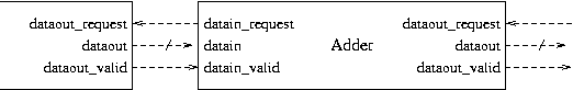
Your entity should be compatible with the component definition in
adder_pkg.vhd.
Measure the total number of logic cells in the design, the throughput
and the latency. Throughput is the maximum clock frequency (MHz). We will
define latency as the number of pipeline register stages, not counting
the first one, times the minimum clock period.
Determine the "cost" with the cost function below but do not attempt
to minimize it.
cost(#logicCells, latency, throughput) = #logicCells * 2/cell
+ latency * 100/ns + 10000MHz / throughput
Supply the following:
-
Timing analyzer results and simulator output from maxplus2
-
Provide one simulation waveform to show your adder adding a few numbers.
-
Cost calculation
Part B: Test Bench
Compile your post-synthesis and layout adder design (*.vho) with the extracted
timing information and the testbench adder_test.vhd, provided. Use the
Mentor Graphics environment. Use the same *.vhd files as in the test bench
exercise for this lab, only substitute your correct pipelined adder from
Part A.
You do not have to write a testbench, or instantiate everything correctly.
As long as your adder.vhd (adder.vho) is compatible with adder_pkg.vhd,
simply compile and simulate as in Exercise, Part C.
Requirements
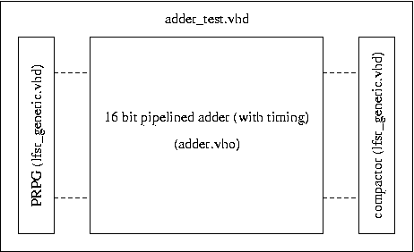
Note: PRPG and Compactor are LFSRs that are already instantiated
by adder_test.vhd.
Synthesize your adder and generate timing-annotated VHDL output (see
exercise and instructions above). For your simulations, use the provided
stimulus signals in adder_test.vhd. This uses initial seed values, chosen
by your TAs for the pseudo-random generators. Run your simulations for
at least 8000 ns. Use a simulation resolution of 'ns'. Display only selected
signals or else you will display thousands of signal traces internal to
the design.
Here is what the testbench stimulus signals test:
-
The testbench simulation tests for correct operation without any pipeline
stalls.
-
Next a pipeline stall from the downstream end is tested.
-
After that, pipeline bubbles are inserted from the upstream end.
Include in your submission for this lab, a timing diagram with the following
signals, as well as any interesting signals in your own design.
Display
the signal values in hexadecimal.
a_internal
b_internal
seed_a
seed_b
sum_internal_x
signature_x
clock
reset
load_prpg
load_compact
serial_prpg_a
serial_prpg_b
serial_compact_x
datain_request_internal
dataout_valid_internal
dataout_request_internal
datain_valid_internal
Extra (for personal satisfaction only)
Show that your VHDL source code (the VHDL code you typed in, in part A)
also simulates with the testbench.
Part C: Testbench Bonus
-
Create and test a testbench that compares your adder to the VHDL "+" operator
and flags errors with assert statements. Try to make use of datain_valid
and dataout_request.